LV5769V 查看數據表(PDF) - ON Semiconductor
零件编号
产品描述 (功能)
生产厂家
LV5769V Datasheet PDF : 9 Pages
| |||
LV5769V
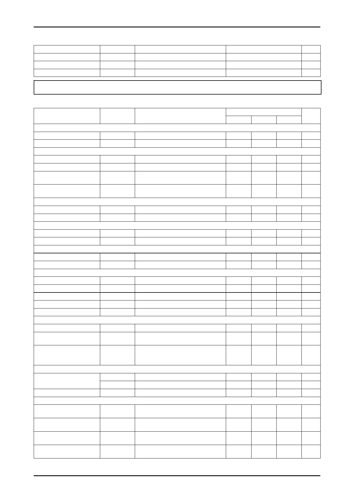
Recommended Operating Conditions at Ta = 25°C
Parameter
Symbol
Conditions
Supply voltage range
Error amplifier input voltage
Oscillatory frequency
VIN
VFB
FOSC
Ratings
Unit
8.5 to 42
V
0 to 1.6
V
80 to 500 kHz
Functional operation above the stresses listed in the Recommended Operating Ranges is not implied. Extended exposure to stresses beyond the Recommended
Operating Ranges limits may affect device reliability.
Electrical Characteristics at Ta = 25°C, VCC = 12V
Parameter
Symbol
Conditions
Reference voltage block
Internal reference voltage
Vref
5V power supply
VDD
Triangular waveform oscillator block
Oscillation frequency
Frequency variation
Oscillation frequency fold back
detection voltage
Oscillation frequency after fold
back
ON/OFF circuit block
FOSC
FOSC DV
VOSC FB
FOSC FB
IC start-up voltage
IC off voltage
Soft start circuit block
VEN on
VEN off
Soft start source current
Soft start sink current
UVLO circuit block
ISS SC
ISS SK
UVLO lock release voltage
UVLO hysteresis
Error amplifier
VUVLO
VUVLO H
Input bias current
Error amplifier gain
Sink output current
Source output current
Current detection amplifier gain
IEA IN
GEA
IEA OSK
IEA OSC
GISNS
over current limiter circuit block
Reference current
Over current detection
comparator offset voltage
Over current detection
comparator common mode
input range
PWM comparator
ILIM
VLIM OFS
Input threshold voltage
(FOSC=125kHz)
Vt max
Vt0
Maximum ON duty
DMAX
Output block
Output stage ON resistance
(the upper side)
Output stage ON resistance
(the under side)
Output stage ON current
(the upper side)
Output stage ON current
(the under side)
RONH
RONL
IONH
IONL
Including offset of E/A
IOUT = 0 to 5mA
RT=220kΩ
VIN = 8.5 to 32V
FB voltage detection after SS ends
EN > 3.5V
EN < 1V, VDD = 5V
FB = 1.0V
FB = 0V
Duty cycle = DMAX
Duty cycle = 0%
Ratings
Unit
min
typ
max
0.654
4.7
0.67
0.686
V
5.2
5.7
V
110
125
1
0.1
1/3FOSC
140 kHz
%
V
kHz
2.5
1.1
4
1000
-10%
-5
VIN-0.45
3.0
1.3
5
2
8
0.7
1400
-100
100
1.5
18.5
3.5
V
1.5
V
6 μA
mA
V
V
100
1800
nA
μA/V
μA
μA
+10% μA
+5 mV
VIN
V
0.9
1.0
1.1
V
0.4
0.5
0.6
V
86
90
95
%
5
Ω
5
Ω
240
mA
240
mA
Continued on next page.
No.A1920-2/9
Share Link: 