LB1860 查看數據表(PDF) - ON Semiconductor
零件编号
产品描述 (功能)
生产厂家
LB1860 Datasheet PDF : 9 Pages
| |||
Specifications
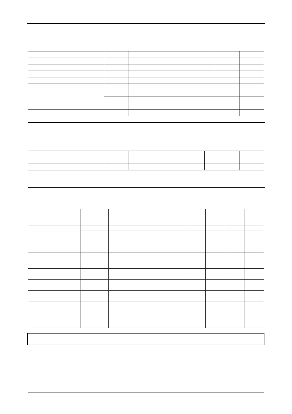
LB1860, LB1860M, LB1861, LB1861M
Absolute Maximum Ratings at Ta = 25 °C, ( ): LB1860M, LB1861M
Parameter
Maximum input current
Output supply voltage
Output current
RD flow-in current
RD supply voltage
Allowable power dissipation
Operating temperature
Storage temperature
Symbol
Conditions
Ratings
Unit
ICC max
VOUT
IOUT
IRD
VRD
Pd1 max
t 20 ms
200
mA
Internal
V
1.5
A
10
mA
50
V
1.1
W
Pd2 max Mounted on 20 15 1.5 mm glass epoxy board
(0.8)
W
Topr
–30 to +80
°C
Tstg
–55 to +125
°C
Stresses exceeding those listed in the Maximum Ratings table may damage the device. If any of these limits are exceeded, device functionality should not be assumed,
damage may occur and reliability may be affected.
Allowable Operating Ranges at Ta = 25 °C
Parameter
Input current range
Common-mode input voltage range
Symbol
ICC
VICM
Conditions
Ratings
Unit
6.0 to 50
mA
0 to VIN –1.5
V
Functional operation above the stresses listed in the Recommended Operating Ranges is not implied. Extended exposure to stresses beyond the Recommended
Operating Ranges limits may affect device reliability.
Electrical Characteristics at Ta = 25 °C, ICC = 10 mA
Parameter
Output limiting voltage
Output saturation voltage
Input voltage
Amp input offset voltage
Amp input bias current
RD output saturation
voltage
C flow-out current
C discharge current
Comparator input threshold
voltage
Ct discharge voltage
Rt input current
Rt comparator voltage
Thermal protection circuit
operating voltage
Thermal protection circuit
hysteresis
Symbol
VOLM1
VO sat1
VO sat2
VO sat3
VIN
VOFF
IBA
VRD (sat)
IC1
IC2
VTH1
VTH2
Vct
IRT
VRT
TSD
Conditions
LB1860, 1860M: IO = 0.1 A
LB1861, 1861M: IO = 0.1 A
IO = 0.5 A
IO = 1.0 A
IO = 1.5 A
ICC = 7.0 mA
IRD = 5 mA
C = GND
C = VIN
VRT = GND
RT = OPEN
Design target
TSD
Design target
min
typ
max
Unit
54
57
60
V
30
32
34
V
0.95
1.2
V
1.15
1.5
V
1.4
2.0
V
6.4
6.7
7.0
V
–7.0
0
7.0
mV
–250
nA
0.15
0.3
V
2.7
3.9
5.0
μA
0.35
0.50 0.65
μA
0.77
0.8 VIN 0.83
V
0.44 0.47 VIN 0.50
V
0.18
0.2 VIN 0.22
V
–440
–350 –240
μA
0.59 0.62 VIN 0.65
V
180
°C
40
°C
Product parametric performance is indicated in the Electrical Characteristics for the listed test conditions, unless otherwise noted. Product performance may not be
indicated by the Electrical Characteristics if operated under different conditions.
www.onsemi.com
2
Share Link: 