APA3160A 查看數據表(PDF) - Anpec Electronics
零件编号
产品描述 (功能)
生产厂家
APA3160A Datasheet PDF : 38 Pages
| |||
APA3160A
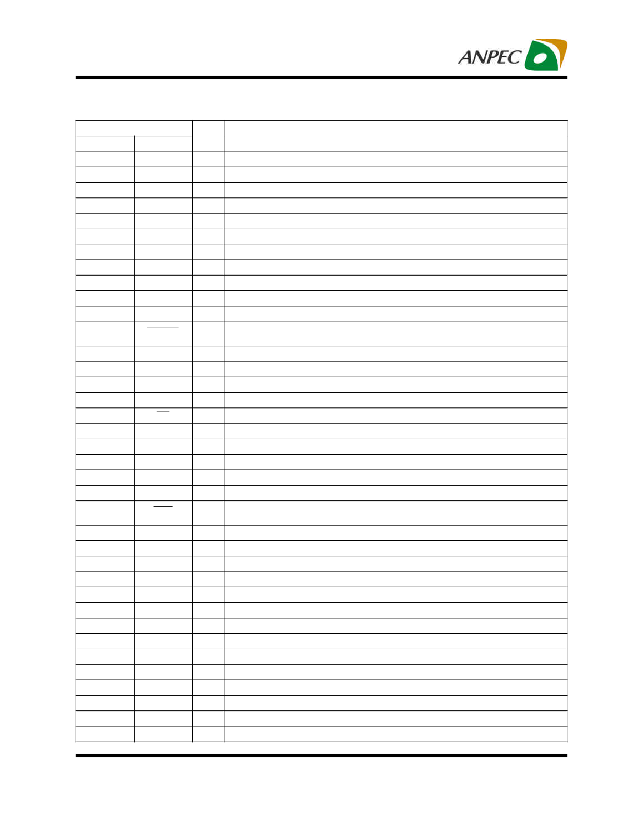
Pin Description
NO.
1
2, 3
4
5, 32
6
7
8
9, 11
10
12
13
PIN
NAME
OUT_A
PVDD_A
ABS
GDREG
NC
TM1
TM2
AVSS
PLL_LF
2V5_AV
AVDD
14
ERROR
15
MCLK
16
TP1
17
TP2
18
2V5_DV
19
SD
20
LRCLK
21
SCLK
22
SDIN
23
SDA
24
SCL
25
RST
26
27
28
29
30
31
33
34, 35
36
37, 38
39
40, 41
42
43
TP3
DVDD
DVSS
GND
AGND
DVREG
DBS
PVDD_D
OUT_D
PGND_CD
OUT_C
PVDD_C
CBS
BBS
I/O/P
FUNCTION
O Output of half bridge A.
P Power supply for half bridge A.
I/O High side bootstrap supply for half bridge A.
O/P Internal regulator output of gate driver.
- No connection.
I Test mode digital input pin.
I Test mode digital input pin.
P Analog power supply’s ground.
O PLL negative loop filter pin.
O/P Internal regulated 2.5V for analog block’s supply, Not for power external device.
P Analog powers supply and connects to 3.3V.
O
When over-temperature, over current over-voltage and under-voltage occur, this pin will
be pull low; and it will be reset to high when the fault condition has be remove.
I Master clock input.
I/O Test mode digital input/output pin.
I/O Test mode digital input/output pin.
O/P Internal regulated 2.5V for digital block’s supply, Not for power external device.
I Active LOW, Shutting down the noise shaper and initiating PWM stop sequence.
I Input serial audio data left/right clock. (Sample rate clock), it’s weak pull down terminal.
I Serial audio data clock (shift clock). SCLK is the serial audio port input data bit clock.
I Serial audio data input.
IO I2C serial control data interface input/output.
I I2C serial control clock input.
I
Reset control, place a logic low to this pin, will reset the APA3160A to its default
condition. It’s weak pull-up terminal.
I/O Test mode digital input/output pin.
P Digital powers supply and connects to 3.3V.
P Digital power supply’s ground.
P Power stage’s analog ground.
P Power stage’s analog ground.
O/P Digital voltage regulator’s output, only for internal used.
I/O High side bootstrap supply for half bridge D.
P Power supply for half bridge D.
O Output of half bridge D.
P Power Ground connection for half bridge C and D.
O Output of half bridge C.
P Power supply for half bridge C.
I/O High side bootstrap supply for half bridge C.
I/O High side bootstrap supply for half bridge B.
Copyright © ANPEC Electronics Corp.
8
Rev. A.6 - Jan., 2013
www.anpec.com.tw
Share Link: 