571MLFT 查看數據表(PDF) - Integrated Device Technology
零件编号
产品描述 (功能)
生产厂家
571MLFT Datasheet PDF : 7 Pages
| |||
ICS571
LOW PHASE NOISE ZERO DELAY BUFFER
ZDB AND MULTIPLIER/DIVIDER
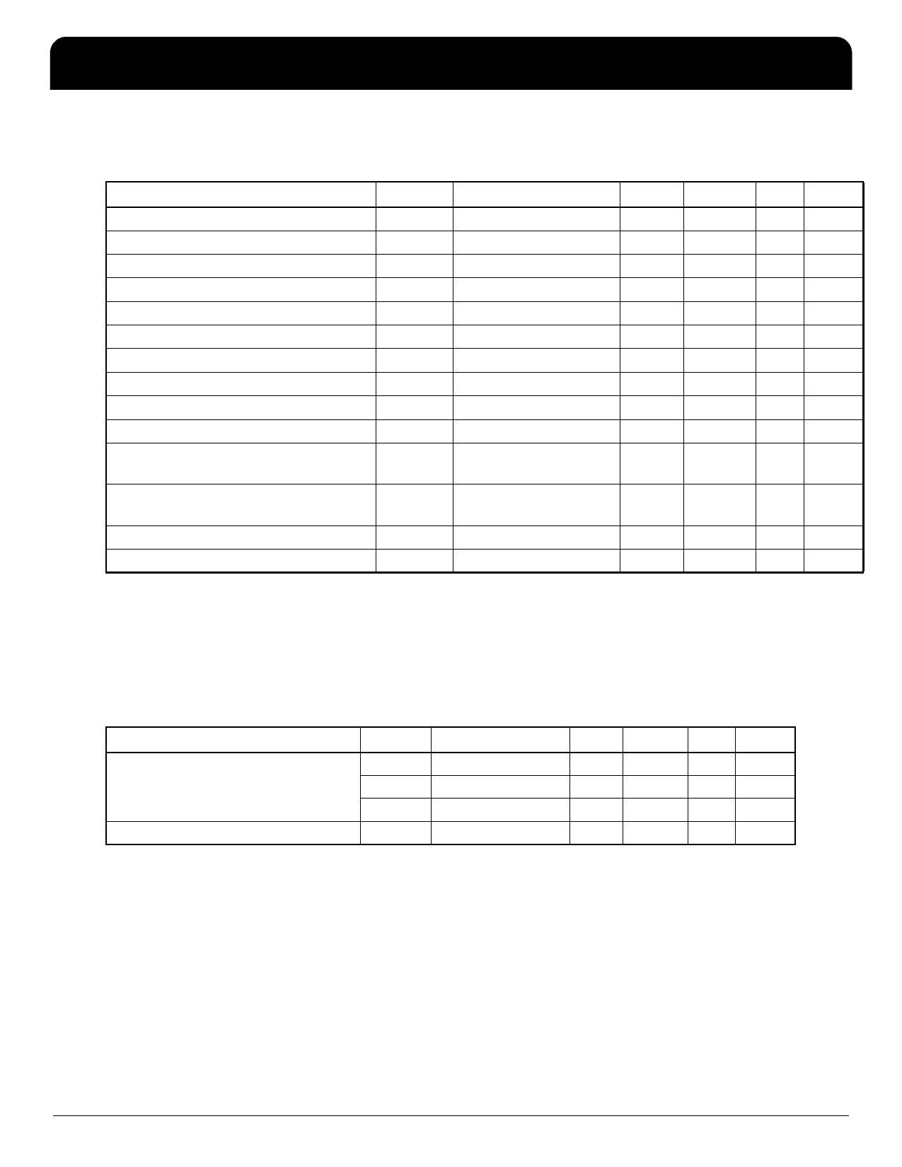
AC Electrical Characteristics
Unless stated otherwise, VDD = 5.0 V or 3.3 V, Ambient Temperature 0 to +70° C
Parameter
Symbol
Conditions
Min.
Input Frequency, clock input
fIN
FB from CLK
20
Input Frequency, clock input
fIN
FB from CLK/2
10
Skew CLK/2 with respect to CLK
Note 2
150
Input clock to output connected to FBIN
Note 2
-500
Output Clock Rise Time, 5 V
0.8 to 2.0 V, 15 pF load
Output Clock Fall Time, 5 V
2.0 to 0.8 V, 15 pF load
Output Clock Rise Time, 3.3 V
0.8 to 2.0 V, 15 pF load
Output Clock Fall Time, 3.3 V
2.0 to 0.8 V, 15 pF load
Input Clock Duty Cycle, 3.3 V
fin = 150 MHz
20
Output Clock Duty Cycle, 3.3 V
At VDD/2
45
Absolute Clock Period Jitter, CLK,
Note 3
Deviation from Mean
One-Sigma Clock Period Jitter, CLK,
Note 3
Phase Noise, Relative to carrier
1 kHz offset
Phase Noise, Relative to carrier
100 kHz offset
Typ. Max. Units
160 MHz
80 MHz
500 850 ps
500 ps
0.3
ns
0.4
ns
0.45
ns
0.55
ns
80
%
49 to 51 55
%
±80
ps
50
ps
-105
-115
dBc/Hz
dBc/Hz
Notes:
1. Sresses beyond these can permanently damage the device.
2. Assumes clocks with the same rise time, measured from rising edges at VDD/2. Measured with 33Ω termination
resistors and 15 pF loads. Applies to both 3.3 V and 5 V operation.
3. CLK/2 has lower jitter (both absolute and one sigma, in ps) than CLK.
Thermal Characteristics
Parameter
Symbol Conditions
Thermal Resistance Junction to
Ambient
θJA Still air
θJA 1 m/s air flow
θJA 3 m/s air flow
Thermal Resistance Junction to Case θJC
Min.
Typ.
Max.
Units
° C/W
° C/W
° C/W
° C/W
IDT™ / ICS™ LOW PHASE NOISE ZERO DELAY BUFFER
5
ICS571
REV H 051310
Share Link: 