ISL85410 查看數據表(PDF) - Renesas Electronics
零件编号
产品描述 (功能)
生产厂家
ISL85410 Datasheet PDF : 21 Pages
| |||
ISL85410
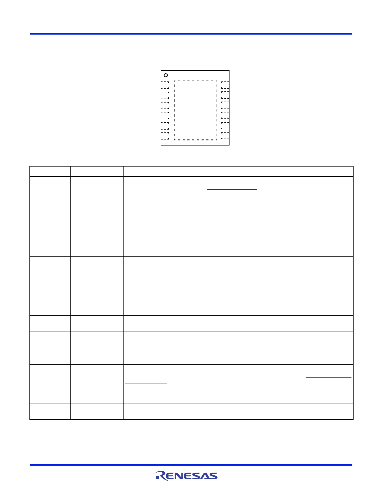
Pin Configuration
ISL85410
(12 LD 4x3 DFN)
TOP VIEW
SS 1
SYNC 2
BOOT 3
VIN 4
PHASE 5
PGND 6
GND
12 FS
11 COMP
10 FB
9 VCC
8 PG
7 EN
Pin Descriptions
PIN NUMBER
1
SYMBOL
SS
2
SYNC
3
4
5
6
7
8
9
10
11
12
EPAD
BOOT
VIN
PHASE
PGND
EN
PG
VCC
FB
COMP
FS
GND
PIN DESCRIPTION
The SS pin controls the soft-start ramp time of the output. A single capacitor from the SS pin to ground
determines the output ramp rate. See “Soft-Start” on page 14 for soft-start details. If the SS pin is tied to
VCC, an internal soft-start of 2ms will be used.
Synchronization and light load operational mode selection input. Connect to logic high or VCC for PWM
mode. Connect to logic low or ground for PFM mode. Logic ground enables the IC to automatically choose
PFM or PWM operation. Connect to an external clock source for synchronization with positive edge trigger.
Sync source must be higher than the programmed IC frequency. There is an internal 5MΩ pull-down resistor
to prevent an undefined logic state if SYNC is left floating.
Floating bootstrap supply pin for the power MOSFET gate driver. The bootstrap capacitor provides the
necessary charge to turn on the internal N-Channel MOSFET. Connect an external 100nF capacitor from this
pin to PHASE.
The input supply for the power stage of the regulator and the source for the internal linear bias regulator.
Place a minimum of 4.7µF ceramic capacitance from VIN to GND and close to the IC for decoupling.
Switch node output. It connects the switching FETs with the external output inductor.
Power ground connection. Connect directly to the system GND plane.
Regulator enable input. The regulator and bias LDO are held off when the pin is pulled to ground. When the
voltage on this pin rises above 1V, the chip is enabled. Connect this pin to VIN for automatic start-up. Do not
connect EN pin to VCC since the LDO is controlled by EN voltage.
Open-drain power-good output that is pulled to ground when the output voltage is below regulation limits or
during the soft-start interval. There is an internal 5MΩ internal pull-up resistor.
Output of the internal 5V linear bias regulator. Decouple to PGND with a 1µF ceramic capacitor at the pin.
Feedback pin for the regulator. FB is the inverting input to the voltage loop error amplifier. COMP is the
output of the error amplifier. The output voltage is set by an external resistor divider connected to FB. In
addition, the PWM regulator’s power-good and UVLO circuits use FB to monitor the regulator output voltage.
COMP is the output of the error amplifier. When it is tied to VCC, internal compensation is used. When only
an RC network is connected from COMP to GND, external compensation is used. See “Loop Compensation
Design” on page 17 for more details.
Frequency selection pin. Tie to VCC for 500kHz switching frequency. Connect a resistor to GND for
adjustable frequency from 300kHz to 2MHz.
Signal ground connections. Connect to application board GND plane with at least 5 vias. All voltage levels
are measured with respect to this pin. The EPAD MUST NOT float.
FN8375 Rev 7.00
March 13, 2015
Page 3 of 21
Share Link: 