74HC14D 查看數據表(PDF) - Nexperia B.V. All rights reserved
零件编号
产品描述 (功能)
生产厂家
74HC14D Datasheet PDF : 18 Pages
| |||
Nexperia
74HC14; 74HCT14
Hex inverting Schmitt trigger
Symbol Parameter Conditions
74HCT14
tpd
propagation nA to nY; see Fig. 6
delay
VCC = 4.5 V
VCC = 5.0 V; CL = 15 pF
tt
transition time VCC = 4.5 V; see Fig. 6
CPD
power
per package;
dissipation
VI = GND to VCC - 1.5 V
capacitance
Tamb = 25 °C
Min Typ Max
Tamb = -40 °C
to +85 °C
Min Max
Tamb = -40 °C Unit
to +125 °C
Min Max
[1]
-
20 34
-
43
-
51 ns
-
17
-
-
-
-
- ns
[2] -
7
15
-
19
-
22 ns
[3] -
8
-
-
-
-
- pF
[1] tpd is the same as tPHL and tPLH.
[2] tt is the same as tTHL and tTLH.
[3] CPD is used to determine the dynamic power dissipation (PD in μW):
PD = CPD × VCC2 × fi × N + Σ (CL × VCC2 × fo) where:
fi = input frequency in MHz;
fo = output frequency in MHz;
CL = output load capacitance in pF;
VCC = supply voltage in V;
N = number of inputs switching;
Σ (CL × VCC2 × fo) = sum of outputs.
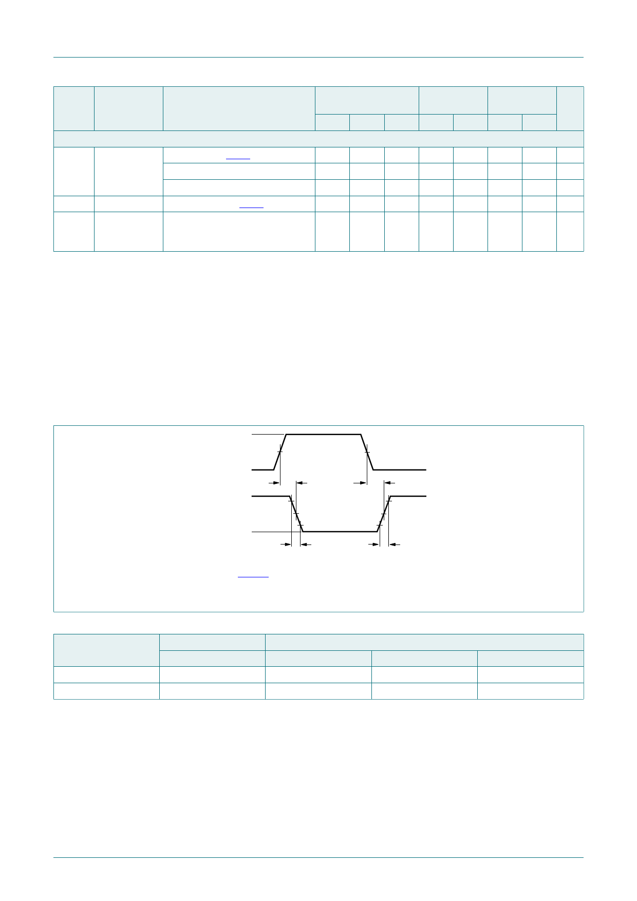
11.1. Waveforms
VI
nA input
GND
VOH
nY output
VOL
VM
t PHL
VM
VM
VM
10 %
t PLH
90 %
Fig. 6.
t THL
t TLH
mna722
Measurement points are given in Table 8.
VOL and VOH are typical voltage output levels that occur with the output load.
Input to output propagation delays
Table 8. Measurement points
Type
Input
74HC14
VM
0.5VCC
74HCT14
1.3 V
Output
VM
0.5VCC
1.3 V
VX
0.1VCC
0.1VCC
VY
0.9VCC
0.9VCC
74HC_HCT14
Product data sheet
All information provided in this document is subject to legal disclaimers.
Rev. 8 — 22 May 2020
© Nexperia B.V. 2020. All rights reserved
6 / 18
Share Link: 