LCE11A 查看數據表(PDF) - New Jersey Semiconductor
零件编号
产品描述 (功能)
生产厂家
LCE11A Datasheet PDF : 2 Pages
| |||
JEIIEU
, Una.
20 STERN AVE.
SPRINGFIELD, NEW JERSEY 07081
U.S.A.
LCE6.5
THRU
LCE28A
TELEPHONE: (973) 376-2922
(212)227-6005
FAX: (973) 376-8960
SERIES
LOW CAPACITANCE TRANSZORB™ TRANSIENT VOLTAGE SUPPRESSOR
Stand-off Voltage - 6.5 to 28 Volts Peak Pulse Power - 1500 Watts
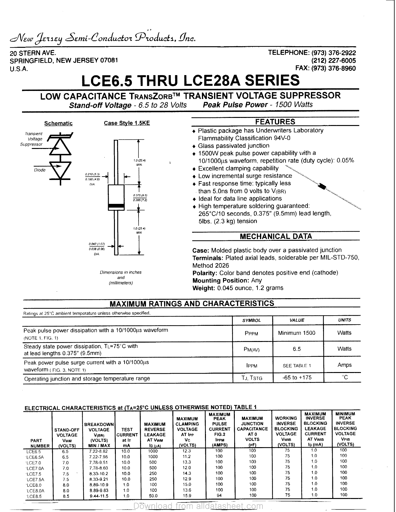
Schematic
Transient
Voltage
Suppressor
Case Style 1.5KE
FEATURES
* Plastic package has Underwriters Laboratory
Flammability Classification 94V-0
* Glass passivated junction
t 1500W peak pulse power capability xvith a
10/1000u,s waveform, repetition rate (duty cycle): 0.05%
4 Excellent clamping capability ^X.
» Low incremental surge resistance %^
» Fast response time; typically less
than 5.0ns from 0 volts to V(BR)
« Ideal for data line applications
* High temperature soldering guaranteed:
265°C/10 seconds, 0.375" (9.5mm) lead length,
5lbs. (2.3 kg) tension
Dimensions in inches
and
(millimeters)
MECHANICAL DATA
Case: Molded plastic body over a passivated junction
Terminals: Plated axial leads, solderable per MIL-STD-750,
Method 2026
Polarity: Color band denotes positive end (cathode)
Mounting Position: Any
Weight: 0.045 ounce, 1.2 grams
MAXIMUM RATINGS AND CHARACTERISTICS
Ratings at 25"C ambient temperature unless otherwise specified.
SYMBOL
VALUE
Peak pulse power dissipation with a 10/1000(.is waveform
{NOTE 1, FIG. 1)
PPPM
Minimum 1500
Steady state power dissipation, Tu=75"C with
at lead lengths 0,375" (9.5mm)
PM(AV)
6.5
Peak power pulse surge current with a 1Q/1QQO[is
waveform ( FIG. 3, NOTE i)
IPPM
SEE TABLE 1
Operating junction and storage temperature range
Tj, TSTG
-65to+175
UNITS
Watts
Watts
Amps
°C
ELECTRICAL CHARACTERISTICS at (TA=25°C UNLESS OTHERWISE NOTED) TABLE 1
PART
NUMBER
1CE6.5
•LCE6.5A
'LCE7.0
LCE7.0A
•LCE7.5
•LCE7.5A
'LCE8.0
1CE8.0A
1CE8.5
STAND-OFF
VOLTAGE
VWM
(VOLTS)
6.5
6.5
7,0
7.0
7.5
7.5
8.0
8.0
8.5
BREAKDOWN
VOLTAGE
TEST
V(BR)
CURRENT
(VOLTS)
at IT
WIN / MAX
mA
7,22-8.82
10.0
7.22-7.98
10.0
7.78-9,51
10.0
7.78-8,60
10.0
8.33-10,2
10.0
8.33-921
10,0
8.89-10.9
1.0
8.89-9,83
1.0
9.44-11.5
1.0
MAXIMUM
REVERSE
LEAKAGE
AT VWM
lo if*i
1000
1000
500
500
250
250
100
100
50.0
MAXIMUM
CLAMPING
VOLTAGE
ATlpp
Vc
(VOLTS)
12.3
11.2
13.3
12.0
14.3
12.9
15.0
13.6
15.9
MAXIMUM
PEAK
PULSE
CURRENT
FIG.2
IPPM
(AMPS)
100
100
100
100
100
100
100
100
94
MAXIMUM
JUNCTION
CAPACITANCE
ATO
VOLTS
(PF)
100
100
100
100
100
100
100
100
100
WORKING
INVERSE
BLOCKING
VOLTAGE
VWIB
(VOLTS)
75
75
75
75
75
75
75
75
75
MAXIMUM
INVERSE
BLOCKING
LEAKAGE
CURRENT
AT VWIB
ID (mA)
1.0
1.0
1.0
1.0
1.0
1,0
1.0
1.0
1.0
MINIMUM
PEAK
INVERSE
BLOCKING
VOLTAGE
VPIB
(VOLTS)
100
100
100
100
100
100
100
100
100
Share Link: 