AD8555 查看數據表(PDF) - Analog Devices
零件编号
产品描述 (功能)
生产厂家
AD8555 Datasheet PDF : 29 Pages
| |||
AD8555
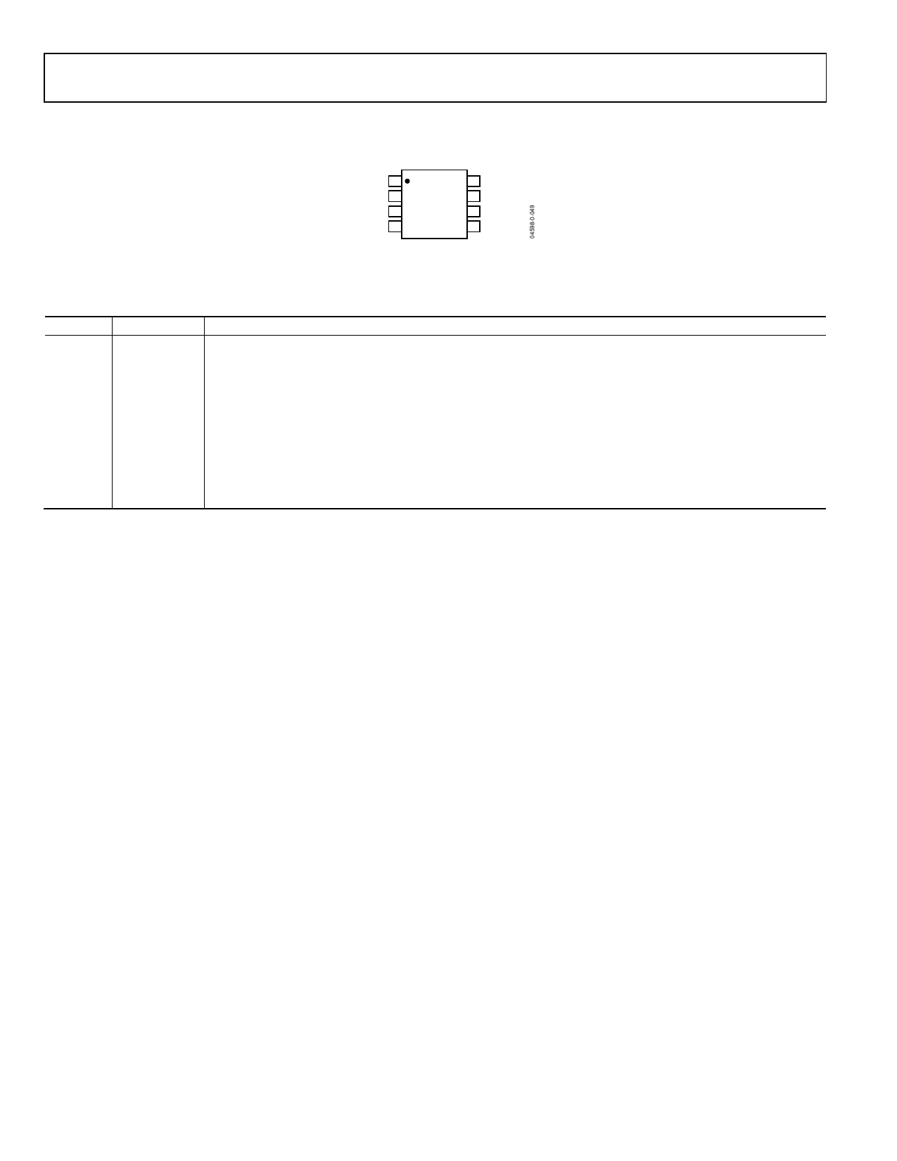
PIN CONFIGURATIONS AND FUNCTION DESCRIPTIONS
VDD 1
8 VSS
FILT/DIGOUT 2 AD8555 7 VOUT
TOP VIEW
DIGIN 3 (Not to Scale) 6 VCLAMP
VNEG 4
5 VPOS
Figure 2. 8-Lead SOIC (Not Drawn to Scale)
Data Sheet
Table 5. 8-Lead SOIC Pin Function Descriptions
Pin No. Mnemonic Description
1
VDD
Positive Supply Voltage.
2
FILT/DIGOUT Unbuffered Amplifier Output In Series with a Resistor RF. Adding a capacitor between FILT and VDD or VSS
implements a low-pass filtering function. In read mode, this pin functions as a digital output.
3
DIGIN
Digital Input.
4
VNEG
Negative Amplifier Input (Inverting Input).
5
VPOS
Positive Amplifier Input (Noninverting Input).
6
VCLAMP
Set Clamp Voltage at Output.
7
VOUT
Buffered Amplifier Output. Buffered version of the signal at the FILT/DIGOUT pin. In read mode, VOUT is a
buffered digital output.
8
VSS
Negative Supply Voltage.
Rev. B | Page 8 of 29
Share Link: 