AD7522J 查看數據表(PDF) - Analog Devices
零件编号
产品描述 (功能)
生产厂家
AD7522J Datasheet PDF : 6 Pages
| |||
instruction fetching by the CPO. When the most significant
2. Diode CR3 on Figure 3 and Figure 4 clamps the ampli-
data byte (DB8 and DB9) is available on the bus, the input
fier junction to -300mV if it attempts to swing negative
buffer is loaded on the positive edge of HBS. The DAC register
during power up or power down. The input structures
updates to the new 10-bit word when LDAC is "high." LDAC
of some high-speed op amps can supply substantial
may be exercised coincident with, or at any time after HBS
current under the transient conditions encountered dur-
(
loads the second byte of data into the input buffer.
ing power sequencing. It is recommended that the PC
SERIAL LOADING
layout be able to accommodate the diodes.
Figure 8 and Figure 9 show the connections and timing
3. Fast op amps will require phase compensation for stability
diagram for serial loading.
due to the pole formed by COUT1 or COUT2 and
w
To load a lO-bit word (SC8 = 1), HBS and LBS must be strobed
RFEEDBACK.
f'
Ii
simultaneously with exactly 10 positive edges to clock the
4. During serial loading, all data inputs (DBO through BD9),
Ii
I
serial data into the input buffer. For 8-bit words (SC8 = 0), only
should be grounded.
It
Ii
8 positive edges are required.
C'
C
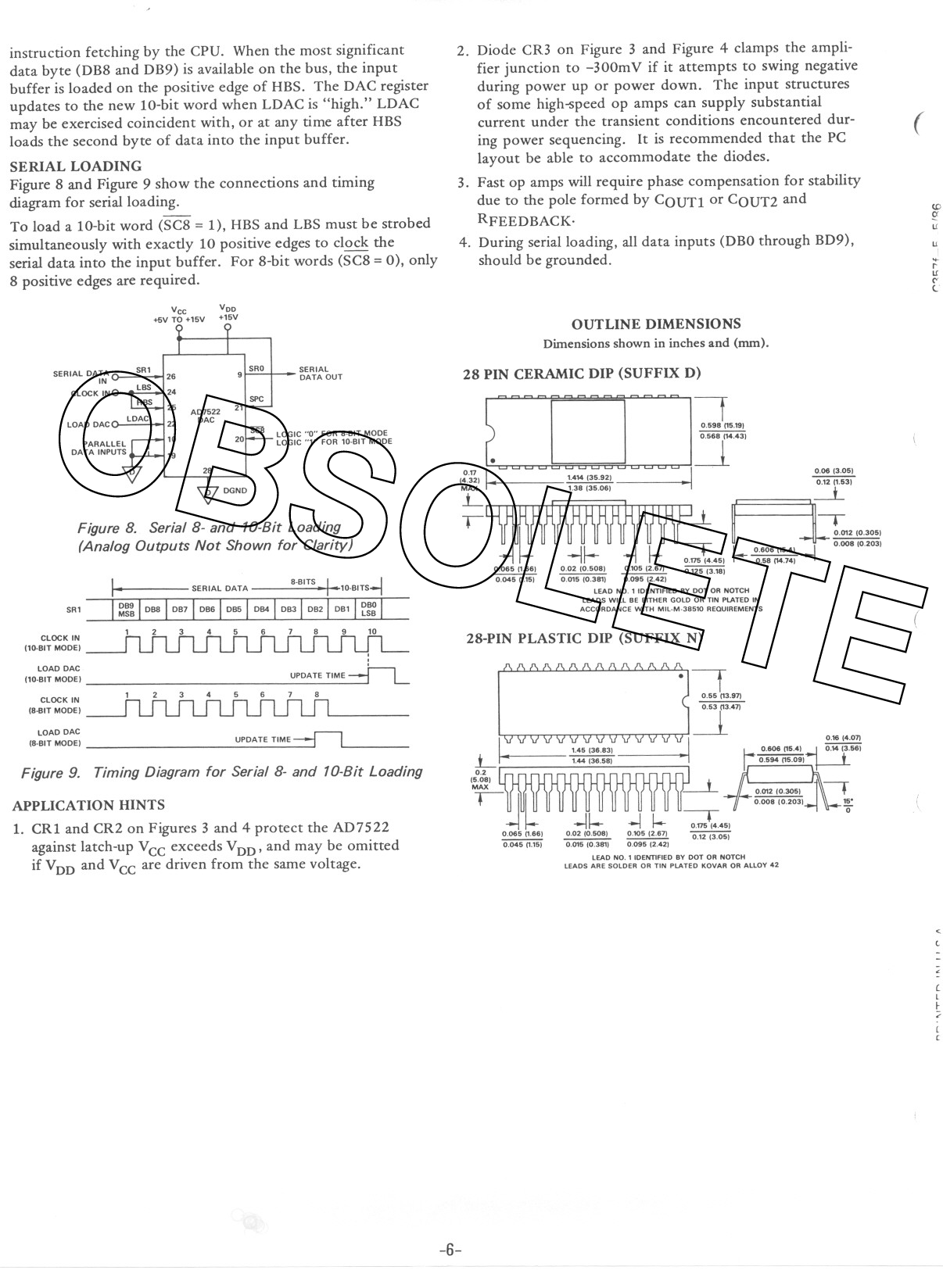
Vcc
VDD
+5VTO +15V +15V
OUTLINE DIMENSIONS
Dimensionsshown in inches and (nun).
OBSOLETE SERIALDATA
IN
CLOCK IN
LOAD DAC
SRI
26
0' SRO
SERIAL
DATA OUT
AD7522
DAC
SPC
21
~
20f---
LOGIC "0" FOR 8.81T MOOE
LOGIC "I" FOR '0.8IT MODE
28 PIN CERAMIC DIP (SUFFIX D)
Figure 8. Serial 8- and to-Bit Loading
(Analog Outputs Not Shown for Clarity)
-.1f-
SERIAL DATA
SR'
CLOCK IN
(lD-BIT MODE)
(
28-PIN PLASTIC DIP (SUFFIX N)
:
LOAD DAC
(IO.BIT MODEl
~
CLOCK IN
(8-8IT MODE)
LOAD DAC
IS-BIT MODEl
7
8
UPDATTElME::::::fl
[~~:::::::~]1: ...~
Figure 9. Timing Diagram for Serial 8- and to-Bit Loading
APPLICATION HINTS
1. CR1 and CR2 on Figures 3 and 4 protect the AD7522
against latch-up Vcc exceeds VDD' and may be omitted
if VDD and Vcc are driven from the same voltage.
LI
15.081
MAX
'0-'2~~I~I~~
~~~~
0.045 ".151
11..444513163.568.)831
..1
~
fIr-~0~.5" "5.091 0.14..68'
0.01210.3051 :--T
-H-- ~ -1
~
~
017514451
~
0.015 10.3811
0.095 12.421
LEAD NO. IIDE""FlEO 8Y DOT OR NOTCH
LEAOS ARE SOLDER OR TIN PLATED KOVAR OR ALLOY 42
(
L
~
;;
- ---
-6-
~
--
- - --
Share Link: 