ADSP-21368KBPZ-3A(RevG) 查看數據表(PDF) - Analog Devices
零件编号
产品描述 (功能)
生产厂家
ADSP-21368KBPZ-3A Datasheet PDF : 62 Pages
| |||
ADSP-21367/ADSP-21368
The memory architecture, in combination with its separate on-
chip buses, allows two data transfers from the core and one
from the I/O processor, in a single cycle.
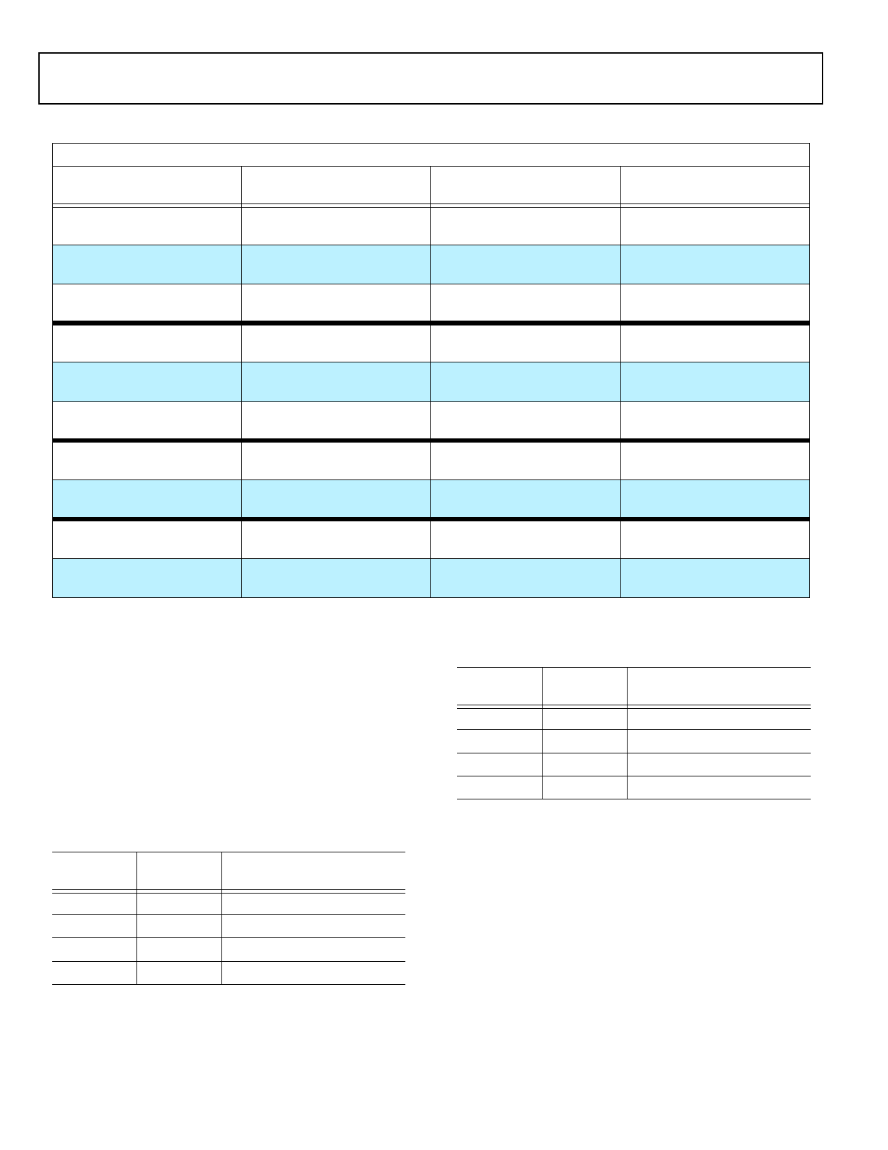
Table 3. Internal Memory Space 1
IOP Registers 0x0000 0000–0x0003 FFFF
Long Word (64 Bits)
Extended Precision Normal or
Instruction Word (48 Bits)
Normal Word (32 Bits)
Short Word (16 Bits)
Block 0 ROM (Reserved)
0x0004 0000–0x0004 BFFF
Block 0 ROM (Reserved)
0x0008 0000–0x0008 FFFF
Block 0 ROM (Reserved)
0x0008 0000–0x0009 7FFF
Block 0 ROM (Reserved)
0x0010 0000–0x0012 FFFF
Reserved
0x0004 F000–0x0004 FFFF
Reserved
0x0009 4000–0x0009 FFFF
Reserved
0x0009 E000–0x0009 FFFF
Reserved
0x0013 C000–0x0013 FFFF
Block 0 SRAM
0x0004 C000–0x0004 EFFF
Block 0 SRAM
0x0009 0000–0x0009 3FFF
Block 0 SRAM
0x0009 8000–0x0009 DFFF
Block 0 SRAM
0x0013 0000–0x0013 BFFF
E Block 1 ROM (Reserved)
0x0005 0000–0x0005 BFFF
Block 1 ROM (Reserved)
0x000A 0000–0x000A FFFF
Block 1 ROM (Reserved)
0x000A 0000–0x000B 7FFF
Block 1 ROM (Reserved)
0x0014 0000–0x0016 FFFF
Reserved
0x0005 F000–0x0005 FFFF
Reserved
0x000B 4000–0x000B FFFF
Reserved
0x000B E000–0x000B FFFF
Reserved
0x0017 C000–0x0017 FFFF
T Block 1 SRAM
0x0005 C000–0x0005 EFFF
Block 1 SRAM
0x000B 0000–0x000B 3FFF
Block 1 SRAM
0x000B 8000–0x000B DFFF
Block 1 SRAM
0x0017 0000–0x0017 BFFF
Block 2 SRAM
E 0x0006 0000–0x0006 0FFF
Block 2 SRAM
0x000C 0000–0x000C 1554
Block 2 SRAM
0x000C 0000–0x000C 1FFF
Block 2 SRAM
0x0018 0000–0x0018 3FFF
Reserved
0x0006 1000– 0x0006 FFFF
Reserved
0x000C 1555–0x000C 3FFF
Reserved
0x000C 2000–0x000D FFFF
Reserved
0x0018 4000–0x001B FFFF
L Block 3 SRAM
0x0007 0000–0x0007 0FFF
Block 3 SRAM
0x000E 0000–0x000E 1554
Block 3 SRAM
0x000E 0000–0x000E 1FFF
Block 3 SRAM
0x001C 0000–0x001C 3FFF
Reserved
O 0x0007 1000–0x0007 FFFF
Reserved
0x000E 1555–0x000F FFFF
Reserved
0x000E 2000–0x000F FFFF
Reserved
0x001C 4000–0x001F FFFF
1 The ADSP-21368 and ADSP-21369 processors include a customer-definable ROM block. Please contact your Analog Devices sales representative for additional details.
S The SRAM can be configured as a maximum of 64k words of
32-bit data, 128k words of 16-bit data, 42k words of 48-bit
instructions (or 40-bit data), or combinations of different word
sizes up to two megabits. All of the memory can be accessed as
16-bit, 32-bit, 48-bit, or 64-bit words. A 16-bit floating-point
B storage format is supported that effectively doubles the amount
of data that can be stored on-chip. Conversion between the
32-bit floating-point and 16-bit floating-point formats is per-
formed in a single instruction. While each memory block can
O store combinations of code and data, accesses are most efficient
when one block stores data using the DM bus for transfers, and
the other block stores instructions and data using the PM bus
for transfers.
On-Chip Memory Bandwidth
The internal memory architecture allows programs to have four
accesses at the same time to any of the four blocks (assuming
there are no block conflicts). The total bandwidth is realized
using the DMD and PMD buses (2x64-bits, core CLK) and the
IOD0/1 buses (2x32-bit, PCLK).
ROM-Based Security
The ADSP-21367/ADSP-21368/ADSP-21369 have a ROM secu-
rity feature that provides hardware support for securing user
software code by preventing unauthorized reading from the
internal code when enabled. When using this feature, the pro-
cessor does not boot-load any external code, executing
Using the DM bus and PM buses, with one bus dedicated to
exclusively from internal ROM. Additionally, the processor is
each memory block, assures single-cycle execution with two
not freely accessible via the JTAG port. Instead, a unique 64-bit
data transfers. In this case, the instruction must be available in
key, which must be scanned in through the JTAG or test access
the cache.
port will be assigned to each customer. The device will ignore a
wrong key. Emulation features and external boot modes are
only available after the correct key is scanned.
Rev. G | Page 6 of 62 | September 2017
Share Link: 