LC79430KNE-E 查看數據表(PDF) - ON Semiconductor
零件编号
产品描述 (功能)
生产厂家
LC79430KNE-E Datasheet PDF : 7 Pages
| |||
LC79430KNE
Specifications
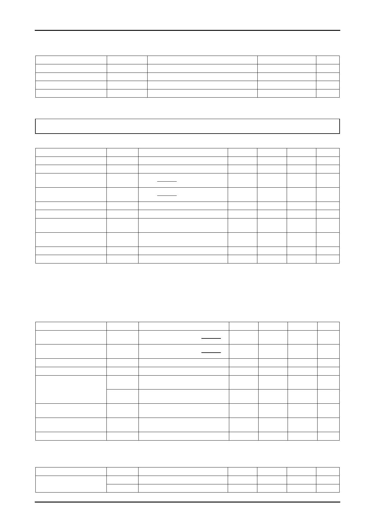
Absolute Maximum Ratings at Ta = 25±2°C, VSS = 0V
Parameter
Symbol
Conditions
Ratings
unit
Maximum supply voltage (Logic) VDD max
-0.3 to +7.0
V
Maximum supply voltage (LCD) VDD-VEE max
*1
0 to 35
V
Maximum input voltage
VI max
-0.3 to VDD+0.3
V
Storage temperature
Tstg
-40 to +125
°C
Note *1 The following relations between elements should be maintained: VDD≥V1>V2>V5>VEE, VDD-V2≤7V,
V5-VEE≤7V
Stresses exceeding Maximum Ratings may damage the device. Maximum Ratings are stress ratings only. Functional operation above the Recommended Operating
Conditions is not implied. Extended exposure to stresses above the Recommended Operating Conditions may affect device reliability.
Allowable Operating Ranges at Ta = -20 to +85°C, VSS = 0V
Parameter
Symbol
Conditions
min
typ
max
unit
Supply voltage (Logic)
VDD
2.7
5.5
V
Supply voltage (LCD)
VDD-VEE
*2, 3
12
32
V
Input high level voltage
VIH
DIO1, DIO80, CP, M, DMIN, MODE,
RS/LS, DISPOFF
0.8VDD
V
Input low level voltage
VIL
DIO1, DIO80, CP, M, DMIN, MODE,
RS/LS, DISPOFF
0.2VDD
V
CP Shift clock
fCP
CP
1 MHz
CP pulse width
tWC
CP
63
ns
Setup time
tSETUP
DIO1 → CP, DIO80 → CP,
100
ns
DMIN → CP
Hold time
tHOLD
DIO1 → CP, DIO80 → CP,
100
ns
DMIN → CP
CP rise time
tR
CP
50
ns
CP fall time
tF
CP
50
ns
Note *2 The following relations between elements should be maintained: VDD≥V1>V2>V5>VEE, VDD-V2≤7V,
V5-VEE≤7V
*3 When the power supply is turned on, power to the LCD driver is turned on after or simultaneously with the
turning on of the logic section’s power supply. When the power supply is turned off, the logic power supply is
turned off after or at the same time the LCD driver power supply is turned off.
Electrical Characteristics at Ta = 25±2°C, VDD = 2.7 to 5.5V
Parameter
Symbol
Conditions
min
typ
max
unit
Input high level current
IIH
VIN=VDD, VDD=5.5V, DIO1, DIO80,
CP, M, DMIN, MODE, RS/LS, DISPOFF
1
μA
Input low level current
IIL
VIN=VSS, VDD=5.5V, DIO1, DIO80,
CP, M, DMIN, MODE, RS/LS, DISPOFF
-1
μA
Output high level voltage
VOH
IOH=-0.4mA, DIO1, DIO80
VDD-0.4
V
Output low level voltage
VOL
IOL=0.4mA, DIO1, DIO80
0.4
V
Driver on resistance
Consumable current drain (1)
Consumable current drain (2)
Input capacitance
RON(1)
RON(2)
ISS
IEE
CI
VDD-VEE=30V, ⎜VDE-VO⎜=0.5V
VDD=4.5V, O1 to O80 *4
VDD-VEE=20V, ⎜VDE-VO⎜=0.5V
VDD=4.5V, O1 to O80 *4
VDD-VEE=30V, CP=14kHz
no-load, VDD=5.5V ; VSS
VDD-VEE=30V, CP=14kHz
no-load, VDD=5.5V ; VEE
f=1MHz ; CP
1.0
kΩ
1.0
kΩ
100
μA
100
μA
8
pF
Note *4 VDE = V1 or V2 or V5 or VEE, V1 = VDD, V2 = 16/17 (VDD-VEE), V5 = 1/17 (VDD-VEE)
Switching Characteristics at Ta = 25±2°C, VSS = 0V, VDD = 2.7 to 5.5V
Parameter
Output delay time
Symbol
Conditions
min
typ
max
unit
tPLH
CL=15pF ; CP → DIO1, CP → DIO80
250
ns
tPHL
CL=15pF ; CP → DIO1, CP → DIO80
250
ns
No. A2123-2/7
Share Link: 