MTSF2P02HD 查看數據表(PDF) - ON Semiconductor
零件编号
产品描述 (功能)
生产厂家
MTSF2P02HD Datasheet PDF : 12 Pages
| |||
MTSF2P02HD
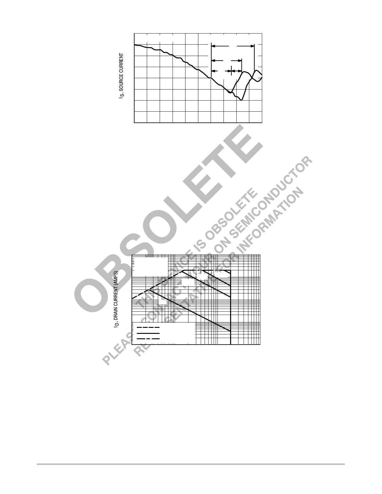
di/dt = 300 A/µs
Standard Cell Density
trr
High Cell Density
trr
tb
ta
t, TIME
Figure 13. Reverse Recovery Time (trr)
SAFE OPERATING AREA
The Forward Biased Safe Operating Area curve (Figure
14) defines the maximum simultaneous drain−to−source
voltage and drain current that a transistor can handle safely
when it is forward biased. Curves are based upon maximum
peak junction temperature and a case temperature (TC) of
25°C. Peak repetitive pulsed power limits are determined by
using the thermal response data in conjunction with the
procedures discussed in AN569, “Transient Thermal
Resistance − General Data and Its Use.”
Switching between the off−state and the on−state may
traverse any load line provided neither rated peak current
(IDM) nor rated voltage (VDSS) is exceeded, and that the
transition time (tr, tf) does not exceed 10 µs. In addition the
total power averaged over a complete switching cycle must
not exceed (TJ(MAX) − TC)/(RθJC).
100
VGS = 8 V
SINGLE PULSE
10 TC = 25°C
1 ms 100 µs
10 ms
1
dc
0.1
0.01
0.1
RDS(on) LIMIT
THERMAL LIMIT
PACKAGE LIMIT
1
10
100
VDS, DRAIN−TO−SOURCE VOLTAGE (VOLTS)
Figure 14. Maximum Rated Forward Biased
Safe Operating Area
http://onsemi.com
7
Share Link: 