HEF4067B-Q100 查看數據表(PDF) - Nexperia B.V. All rights reserved
零件编号
产品描述 (功能)
生产厂家
HEF4067B-Q100 Datasheet PDF : 17 Pages
| |||
Nexperia
HEF4067B-Q100
16-channel analog multiplexer/demultiplexer
9,
(LQSXW
9
9''
<QRU=RXWSXW
92/
92+
<QRU=RXWSXW
9
90
W3/=
W3+=
9;
9<
90
W3=/
90
W3=+
90
VZLWFK21
VZLWFK2))
VZLWFK21
DDJ
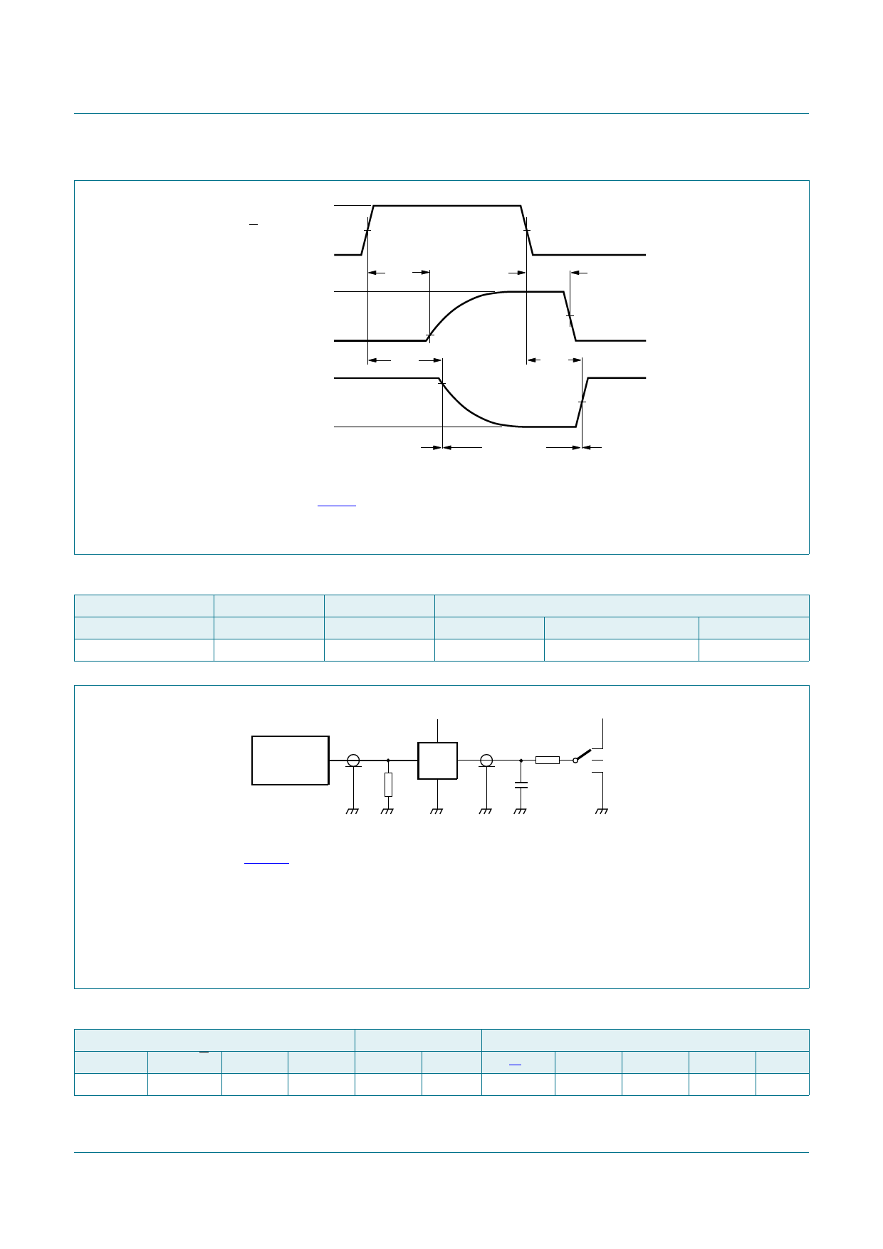
Measurement points are shown in Table 9.
VOL and VOH are typical output voltage levels that occur with the output load.
Fig 11. Enable and disable times
Table 9. Measurement points
Supply voltage
Input
VCC
5 V to 15 V
VM
0.5VDD
VI
GND to VDD
Output
VM
0.5VDD
VX
10%
VY
90%
38/6(
9,
*(1(5$725
9''
92
'87
57
9''
5/ 6
&/
RSHQ
DDJ
Test data is given in Table 10.
Definitions test circuit:
RT = termination resistance should be equal to output impedance Zo of the pulse generator
CL = load capacitance including jig and probe capacitance
RL = load resistor
S1 = test selection switch
Fig 12. Test circuit for measuring switching times
Table 10. Test data
Input
Yn, Z
An and E tr, tf
VDD or VSS VDD or VSS 20 ns
VM
0.5VDD
Load
CL
50 pF
RL
10 k
S1 position
tPHL[1]
tPLH
VDD or VSS VSS
tPZH, tPHZ tPZL, tPLZ other
VSS
VDD
VSS
[1] For Yn to Z or Z to Yn propagation delays, use VSS. For An or to Yn or Z propagation delays, use VDD.
HEF4067B_Q100
Product data sheet
All information provided in this document is subject to legal disclaimers.
Rev. 2 — 11 September 2014
© Nexperia B.V. 2017. All rights reserved
10 of 17
Share Link: 