PCF2123U/10AA/1 查看數據表(PDF) - NXP Semiconductors.
零件编号
产品描述 (功能)
生产厂家
PCF2123U/10AA/1 Datasheet PDF : 64 Pages
| |||
NXP Semiconductors
PCF2123
SPI Real time clock/calendar
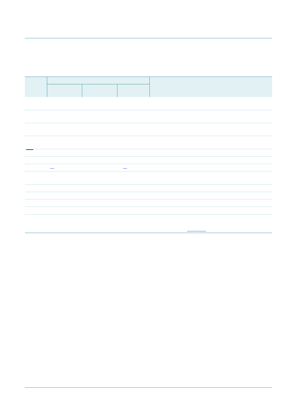
7.2 Pin description
Table 4.
Symbol
OSCI
Pin description
Pin
HVQFN16
TSSOP14
PCF2123Ux
(PCF2123BS/1) (PCF2123TS/1) (bare die)
16
1
7
OSCO 1
2
8
n.c.
6, 7, 14, 15
3, 11
-
TEST 2
4
9
INT
3
5
CE
4
6
VSS
5[1]
7
SDO
8
8
10
11
12[2]
1
SDI
9
9
2
SCL
10
10
3
CLKOE 11
12
4
CLKOUT 12
13
5
VDD
13
14
6
Description
oscillator input; high-impedance node; minimize wire length
between quartz and package
oscillator output; high-impedance node; minimize wire length
between quartz and package
do not connect and do not use as feed through; connect to
VDD if floating pins are not allowed
test pin; not user accessible; connect to VSS or leave floating
(internally pulled down)
interrupt output (open-drain; active LOW)
chip enable input (active HIGH) with internal pull down
ground
serial data output, push-pull; high-impedance when not
driving; can be connected to SDI for single wire data line
serial data input; may float when CE is inactive
serial clock input; may float when CE is inactive
CLKOUT enable or disable pin; enable is active HIGH
clock output (open-drain)
supply voltage; positive or negative steps in VDD may affect
oscillator performance; recommend 100 nF decoupling close
to the device (see Figure 30)
[1] The die paddle (exposed pad) is wired to VSS and should be electrically isolated.
[2] The substrate (rear side of the die) is wired to VSS and should be electrically isolated.
PCF2123
Product data sheet
All information provided in this document is subject to legal disclaimers.
Rev. 6 — 15 July 2013
© NXP B.V. 2013. All rights reserved.
5 of 64
Share Link: 