PCF8564ACX9 查看數據表(PDF) - NXP Semiconductors.
零件编号
产品描述 (功能)
生产厂家
PCF8564ACX9 Datasheet PDF : 45 Pages
| |||
NXP Semiconductors
7. Pinning information
7.1 Pinning
PCF8564A
Real time clock and calendar
OSCI 1
OSCO 2
INT 3
VSS 4
9 CLKOE
y
x
0,0
PCF8564AU
8 VDD
7 CLKOUT
6 SCL
5 SDA
OSCI 1
OSCO 2
INT 3
VSS 4
8
y
x
0,0
PCF8564ACX
9 CLKOE
VDD
7 CLKOUT
6 SCL
5 SDA
013aaa032
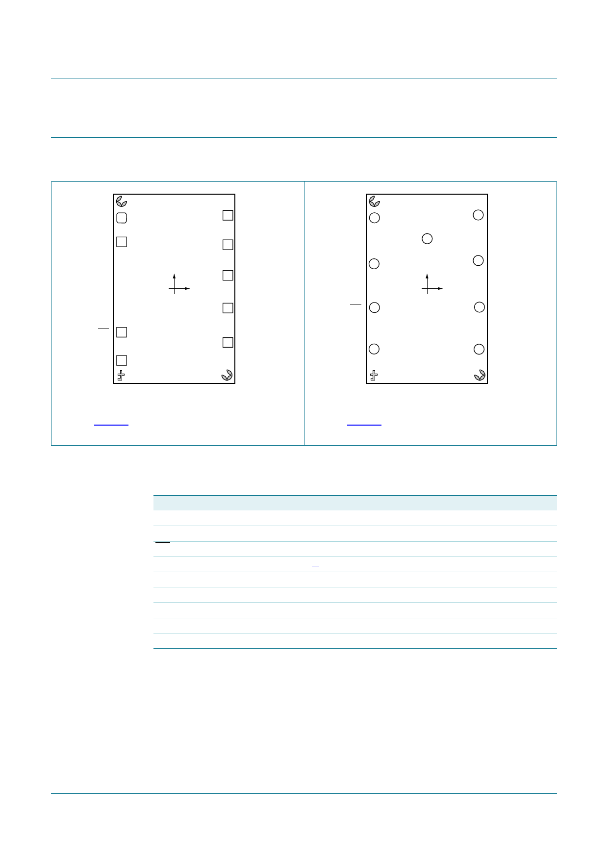
Fig 2.
Viewed from pad side. For mechanical details, see
Figure 27.
Pinning diagram of PCF8564AU
013aaa033
Fig 3.
Viewed from bump side. For mechanical details, see
Figure 28.
Pinning diagram of PCF8564ACX9
7.2 Pin description
Table 3. Pin description
Symbol
Pin
OSCI
1
OSCO
2
INT
3
VSS
4
SDA
5
SCL
6
CLKOUT
7
VDD
8
CLKOE
9
Description
oscillator input
oscillator output
interrupt output, open-drain, active LOW
ground[1]
serial data input and output
serial clock input
clock output, push-pull
supply voltage
CLKOUT output enable
[1] The substrate (rear side of the die) is wired to VSS but should not be electrically contacted.
PCF8564A
Product data sheet
All information provided in this document is subject to legal disclaimers.
Rev. 02 — 30 September 2010
© NXP B.V. 2010. All rights reserved.
4 of 45
Share Link: 