PCA9554PW,118 查看數據表(PDF) - NXP Semiconductors.
零件编号
产品描述 (功能)
生产厂家
PCA9554PW,118 Datasheet PDF : 35 Pages
| |||
NXP Semiconductors
PCA9554; PCA9554A
8-bit I2C-bus and SMBus I/O port with interrupt
6.1.4 Register 2 - Polarity Inversion register
This register allows the user to invert the polarity of the Input Port register data. If a bit in
this register is set (written with ‘1’), the corresponding Input Port data is inverted. If a bit in
this register is cleared (written with a ‘0’), the Input Port data polarity is retained.
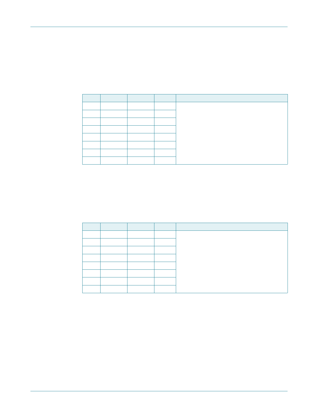
Table 7. Register 2 - Polarity Inversion register bit description
Legend: * default value.
Bit Symbol Access Value Description
7
N7
R/W
0*
inverts polarity of Input Port register data
6
N6
5
N5
R/W
0*
R/W
0*
0 = Input Port register data retained (default value)
1 = Input Port register data inverted
4
N4
R/W
0*
3
N3
R/W
0*
2
N2
R/W
0*
1
N1
R/W
0*
0
N0
R/W
0*
6.1.5 Register 3 - Configuration register
This register configures the directions of the I/O pins. If a bit in this register is set, the
corresponding port pin is enabled as an input with high-impedance output driver. If a bit in
this register is cleared, the corresponding port pin is enabled as an output. At reset, the
I/Os are configured as inputs with a weak pull-up to VDD.
Table 8. Register 3 - Configuration register bit description
Legend: * default value.
Bit Symbol Access Value Description
7
C7
R/W
1*
configures the directions of the I/O pins
6
C6
5
C5
4
C4
R/W
1*
R/W
1*
R/W
1*
0 = corresponding port pin enabled as an output
1 = corresponding port pin configured as input
(default value)
3
C3
R/W
1*
2
C2
R/W
1*
1
C1
R/W
1*
0
C0
R/W
1*
6.2 Power-on reset
When power is applied to VDD, an internal Power-On Reset (POR) holds the
PCA9554/PCA9554A in a reset condition until VDD has reached VPOR. At that point, the
reset condition is released and the PCA9554/PCA9554A registers and state machine will
initialize to their default states. Thereafter, VDD must be lowered below 0.2 V to reset the
device.
For a power reset cycle, VDD must be lowered below 0.2 V and then restored to the
operating voltage.
PCA9554_9554A
Product data sheet
All information provided in this document is subject to legal disclaimers.
Rev. 10 — 8 November 2017
© NXP Semiconductors N.V. 2017. All rights reserved.
8 of 35
Share Link: 