PCA9554 查看數據表(PDF) - ON Semiconductor
零件编号
产品描述 (功能)
生产厂家
PCA9554 Datasheet PDF : 11 Pages
| |||
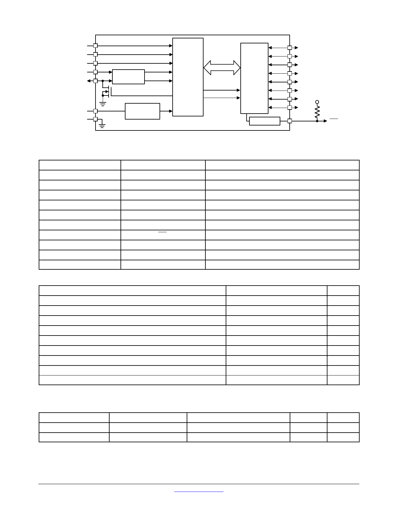
PCA9554
A0
A1
A2
SCL
SDA
VCC
VSS
INPUT
FILTER
POWER−ON
RESET
8−BIT
I2C/SMBUS
CONTROL
WRITE pulse
READ pulse
INPUT/
OUTPUT
PORTS
LP FILTER
I/O0
I/O1
I/O2
I/O3
I/O4
I/O5
I/O6 VCC
I/O7
INT
Table 1. PIN DESCRIPTION
TSSOP
1
2
3
4−7
8
9−12
13
14
15
16
Figure 1. Block Diagram
Note: All I/Os are set to inputs at RESET.
Pin Name
A0
A1
A2
I/O0−3
VSS
I/O4−7
INT
SCL
SDA
VCC
Function
Address Input 0
Address Input 1
Address Input 2
Input/Output Port 0 to Input/Output Port 3
Ground
Input/Output Port 4 to Input/Output Port 7
Interrupt Output (open drain)
Serial Clock
Serial Data
Power Supply
Table 2. ABSOLUTE MAXIMUM RATINGS
Parameters
Ratings
Units
VCC with Respect to Ground
Voltage on Any Pin with Respect to Ground
−0.5 to +6.5
V
−0.5 to +5.5
V
DC Current on I/O0 to I/O7
DC Input Current
±50
mA
±20
mA
VCC Supply Current
VSS Supply Current
Package Power Dissipation Capability (TA = 25°C)
Junction Temperature
85
mA
100
mA
1.0
W
+150
°C
Storage Temperature
−65 to +150
°C
Stresses exceeding those listed in the Maximum Ratings table may damage the device. If any of these limits are exceeded, device functionality
should not be assumed, damage may occur and reliability may be affected.
Table 3. RELIABILITY CHARACTERISTICS
Symbol
Parameter
Reference Test Method
VZAP (Note 2)
ESD Susceptibility
JEDEC Standard JESD 22
ILTH (Notes 2, 3)
Latch−up
JEDEC Standard 17
2. This parameter is tested initially and after a design or process change that affects the parameter.
3. Latch−up protection is provided for stresses up to 100 mA on address and data pins from −1 V to VCC +1 V.
Min
2000
100
Units
Volts
mA
www.onsemi.com
2
Share Link: 