PCA9554 查看數據表(PDF) - ON Semiconductor
零件编号
产品描述 (功能)
生产厂家
PCA9554 Datasheet PDF : 11 Pages
| |||
PCA9554
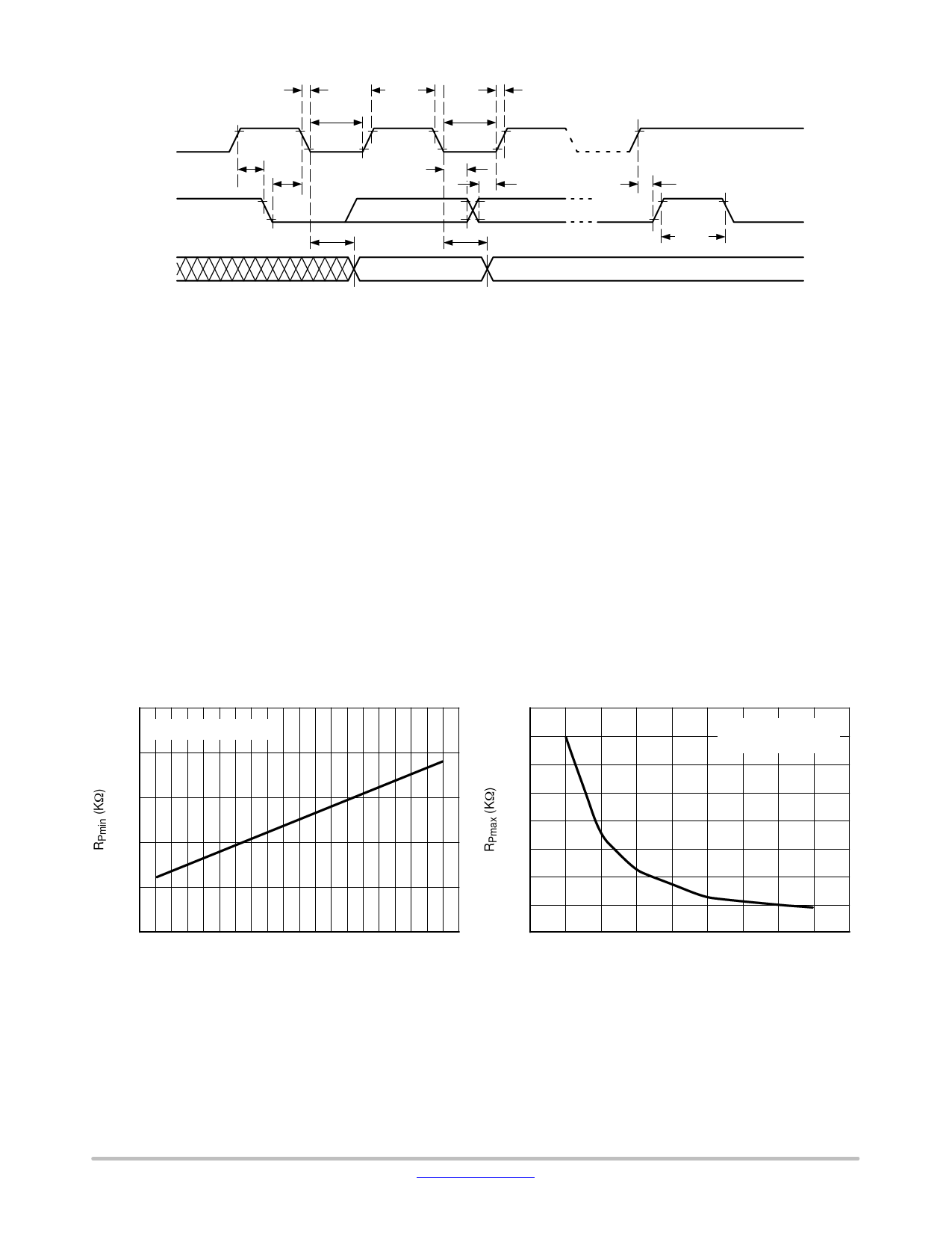
tF
tHIGH
tR
tLOW
tLOW
SCL
tSU:STA
SDA IN
tHD:STA
tHD:DAT
tSU:DAT
SDA OUT
tAA
tDH
tSU:STO
tBUF
Figure 2. I2C Serial Interface Timing
Pin Description
SCL: Serial Clock
The serial clock input clocks all data transferred into or out
of the device. The SCL line requires a pull−up resistor if it
is driven by an open drain output.
SDA: Serial Data/Address
The bidirectional serial data/address pin is used to transfer
all data into and out of the device. The SDA pin is an open
drain output and can be wire−ORed with other open drain or
open collector outputs. A pull−up resistor must be connected
from SDA line to VCC. The value of the pull−up resistor, RP,
can be calculated based on minimum and maximum values
from Figure 3 and Figure 4 (see Note).
A0, A1, A2: Device Address Inputs
These inputs are used for extended addressing capability.
The A0, A1, A2 pins should be hardwired to VCC or VSS.
When hardwired, up to eight PCA9554s may be addressed
on a single bus system. The levels on these inputs are
compared with corresponding bits, A2, A1, A0, from the
slave address byte.
I/O0 to I/O7: Input / Output Ports
Any of these pins may be configured as input or output.
The simplified schematic of I/O0 to I/O7 is shown in
Figure 5. When an I/O is configured as an input, the Q1 and
Q2 output transistors are off creating a high impedance input
with a weak pull−up resistor (typical 100 kW). If the I/O pin
is configured as an output, the push−pull output stage is
enabled. Care should be taken if an external voltage is
applied to an I/O pin configured as an output due to the low
impedance paths that exist between the pin and either VCC
or VSS.
2.5
IOL = 3 mA @ VOLmax
2.0
8
7
Fast Mode I2C Bus /
tr max − 300 ns
6
1.5
5
4
1.0
3
2
0.5
1
0
2.0 2.4 2.8 3.2 3.6 4.0 4.4 4.8 5.2 5.6
0
0 50 100 150 200 250 300 350 400
VCC (V)
CBUS (pF)
NOTE:
Figure 3. Minimum RP Value vs.
Supply Voltage
Figure 4. Maximum RP Value vs.
Bus Capacitance
According to the Fast Mode I2C bus specification, for bus capacitance up to 200 pF, the pull up device can be a resistor. For bus
loads between 200 pF and 400 pF, the pull−up device can be a current source (Imax = 3 mA) or a switched resistor circuit.
www.onsemi.com
5
Share Link: 