PCA9554 查看數據表(PDF) - ON Semiconductor
零件编号
产品描述 (功能)
生产厂家
PCA9554 Datasheet PDF : 11 Pages
| |||
PCA9554
Functional Description
The PCA9554’s general purpose input/output (GPIO)
peripherals provide up to eight I/O ports, controlled through
an I2C compatible serial interface.
The PCA9554 supports the I2C Bus data transmission
protocol. This I2C Bus protocol defines any device that
sends data to the bus to be a transmitter and any device
receiving data to be a receiver. The transfer is controlled by
the Master device which generates the serial clock and all
START and STOP conditions for bus access. The PCA9554
operates as a Slave device. Both the Master device and Slave
device can operate as either transmitter or receiver, but the
Master device controls which mode is activated.
I2C Bus Protocol
The features of the I2C bus protocol are defined as follows:
1. Data transfer may be initiated only when the bus is
not busy.
2. During a data transfer, the data line must remain
stable whenever the clock line is high. Any
changes in the data line while the clock line is high
will be interpreted as a START or STOP condition
(Figure 6).
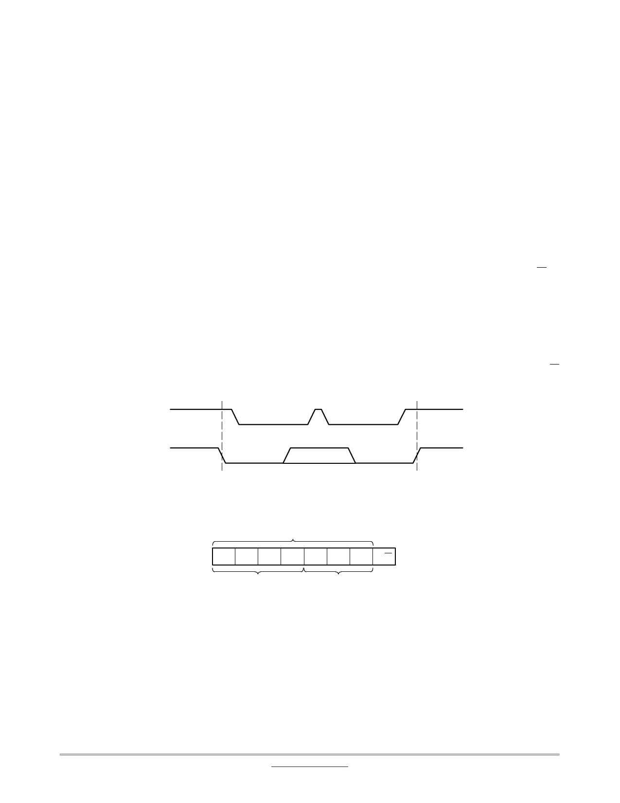
START and STOP Conditions
The START Condition precedes all commands to the
device, and is defined as a HIGH to LOW transition of SDA
when SCL is HIGH. The PCA9554 monitors the SDA and
SCL lines and will not respond until this condition is met.
A LOW to HIGH transition of SDA when SCL is HIGH
determines the STOP condition. All operations must end
with a STOP condition.
Device Addressing
After the bus Master sends a START condition, a slave
address byte is required to enable the PCA9554 for a read or
write operation. The four most significant bits of the slave
address are fixed as binary 0100 for the PCA9554 (Figure 7).
The PCA9554 uses the next three bits as address bits.
The address bits A2, A1 and A0 are used to select which
device is accessed from maximum eight devices on the same
bus. These bits must compare to their hardwired input pins.
The 8th bit following the 7−bit slave address is the R/W bit
that specifies whether a read or write operation is to be
performed. When this bit is set to “1”, a read operation is
initiated, and when set to “0”, a write operation is selected.
Following the START condition and the slave address
byte, the PCA9554 monitors the bus and responds with an
acknowledge (on the SDA line) when its address matches
the transmitted slave address. The PCA9554 then performs
a read or a write operation depending on the state of the R/W
bit.
SCL
SDA
START
CONDITION
Figure 6. START/STOP Condition
STOP
CONDITION
SLAVE ADDRESS
0 1 0 0 A2 A1 A0 R/W
FIXED
PROGRAMMABLE
HARDWARE
SELECTABLE
Figure 7. PCA9554 Slave Address
www.onsemi.com
7
Share Link: 