PCA9554 查看數據表(PDF) - ON Semiconductor
零件编号
产品描述 (功能)
生产厂家
PCA9554 Datasheet PDF : 11 Pages
| |||
PCA9554
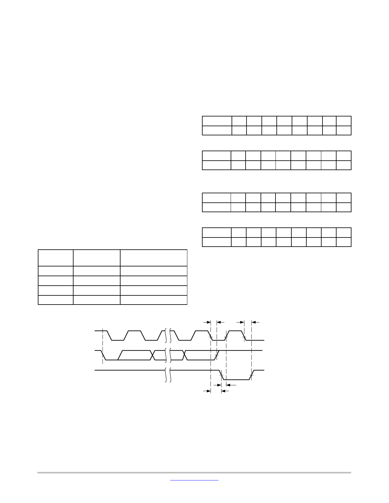
Acknowledge
After a successful data transfer, each receiving device is
required to generate an acknowledge. The acknowledging
device pulls down the SDA line during the ninth clock cycle,
signaling that it received the 8 bits of data. The SDA line
remains stable LOW during the HIGH period of the
acknowledge related clock pulse (Figure 6).
The PCA9554 responds with an acknowledge after
receiving a START condition and its slave address. If the
device has been selected along with a write operation, it
responds with an acknowledge after receiving each 8−bit
byte.
When the PCA9554 begins a READ mode it transmits 8
bits of data, releases the SDA line, and monitors the line for
an acknowledge. Once it receives this acknowledge, the
PCA9554 will continue to transmit data. If no acknowledge
is sent by the Master, the device terminates data transmission
and waits for a STOP condition. The master must then issue
a STOP condition to return the PCA9554 to the standby
power mode and place the device in a known state.
Registers and Bus Transactions
The PCA9554 consists of an input port register, an output
port register, a polarity inversion register and a
configuration register. Table 7 shows the register address
table. Tables 8 to 11 list Register 0 through Register 3
information.
Table 7. REGISTER COMMAND BYTE
Command
(hex)
Protocol
Function
0x00
Read byte
Input port register
0x01
Read/write byte
Output port register
0x02
Read/write byte Polarity inversion register
0x03
Read/write byte
Configuration register
The command byte is the first byte to follow the device
address byte during a write/read bus transaction. The
register command byte acts as a pointer to determine which
register will be written or read.
The input port register is a read only port. It reflects the
incoming logic levels of the I/O pins, regardless of whether
the pin is defined as an input or an output by the
configuration register. Writes to the input port register are
ignored.
Table 8. REGISTER 0 – INPUT PORT REGISTER
bit
I7
I6
I5
I4
I3
I2
I1
I0
default 1 1 1 1 1 1 1 1
Table 9. REGISTER 1 – OUTPUT PORT REGISTER
bit
O7 O6 O5 O4 O3 O2 O1 O0
default 1 1 1 1 1 1 1 1
Table 10. REGISTER 2 –
POLARITY INVERSION REGISTER
bit
N7 N6 N5 N4 N3 N2 N1 N0
default 0 0 0 0 0 0 0 0
Table 11. REGISTER 3 – CONFIGURATION REGISTER
bit
C7 C6 C5 C4 C3 C2 C1 C0
default 1 1 1 1 1 1 1 1
SCL FROM
MASTER
BUS RELEASE DELAY (TRANSMITTER)
1
8
BUS RELEASE DELAY (RECEIVER)
9
DATA OUTPUT
FROM TRANSMITTER
DATA OUTPUT
FROM RECEIVER
START
ACK DELAY
ACK SETUP
Figure 8. Acknowledge Timing
www.onsemi.com
8
Share Link: 