42552 查看數據表(PDF) - Peregrine Semiconductor Corp.
零件编号
产品描述 (功能)
生产厂家
42552 Datasheet PDF : 9 Pages
| |||
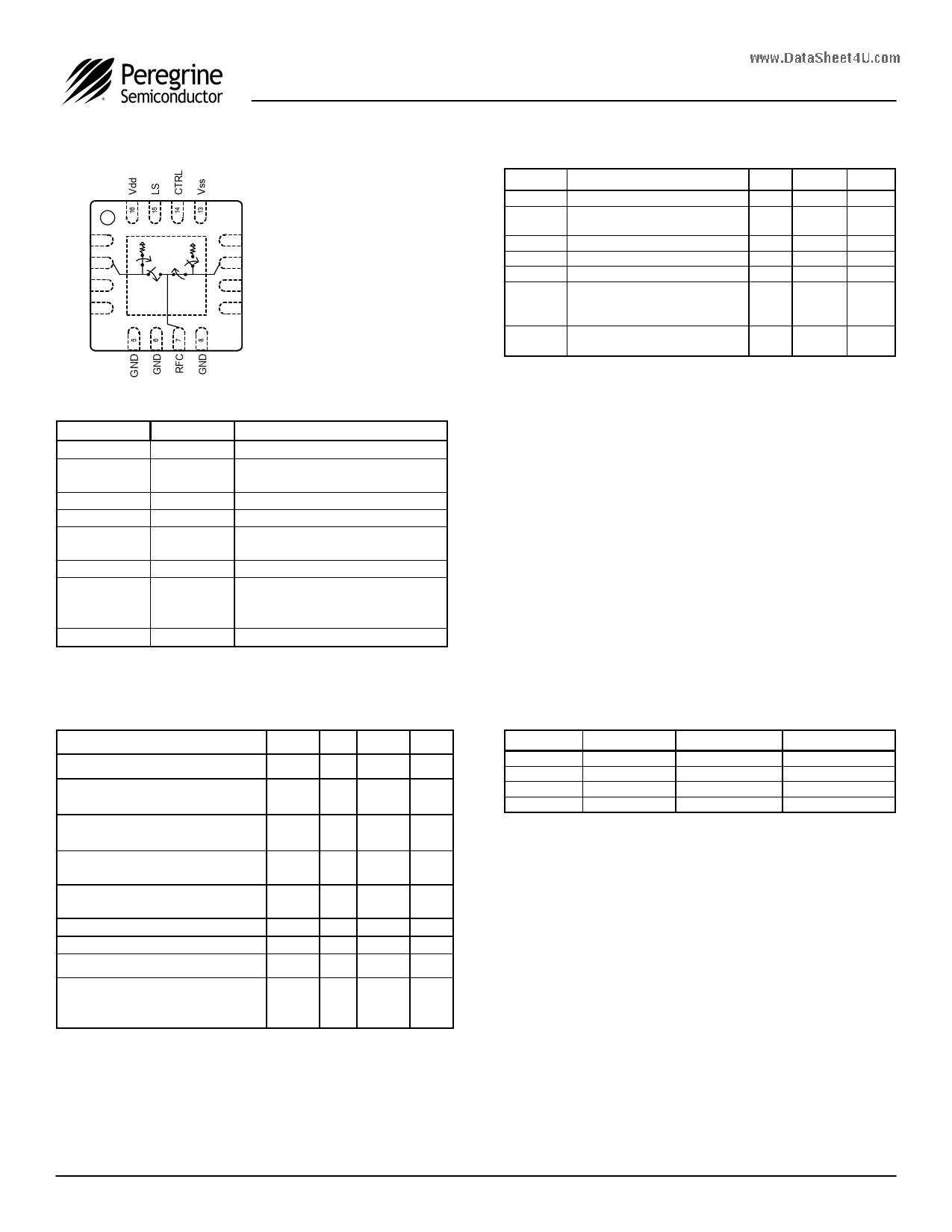
Figure 3. Pin Configuration (Top View)
GND 1
RF1 2
GND 3
GND 4
12 GND
11 RF2
10 GND
9 GND
Table 2. Pin Descriptions
Pin No. Pin Name
Description
2
RF1
RF Port 1
1, 3, 4, 5, 6,
8, 9, 10, 12
GND
Ground
7
RFC
RF Common
11
RF2
RF Port 2
13
VSS
Negative supply voltage or GND
connection (Note 1)
14
CTRL
CMOS level:
Logic Select - Used to determine
15
LS
the definition for the CTRL pin (see
Table 5)
16
VDD
Nominal 3.3 V supply connection
Note: 1. Use VSS (pin 13, VSS = -VDD) to bypass and disable
internal negative voltage generator. Connect VSS (pin 13) to GND
(VSS = 0V) to enable internal negative voltage generator.
Table 3. Operating Ranges
www.DataSheePt4aUra.cmometer
VDD Positive Power Supply Voltage
VSS Negative Power Supply Voltage
(external power supply used)
Min Typ Max Units
3.0 3.3 3.6
V
-3.6 -3.3 -3.0
V
VSS Negative Power Supply Voltage
(internal power supply used)
-0.1
0.0
0.0
V
IDD Power Supply Current
(VSS = 0V, Temp = +85 °C)
ISS Negative Supply
(VSS = -VDD, Temp = 25 °C)
Control Voltage High
Control Voltage Low
15 120 µA
-10 -40 µA
0.7xVDD
V
0.3xVDD V
TOP Operating temperature range
-40 25 85
°C
RF Power In1(PIN):
9 kHz ≤ 1 MHz
1 MHz ≤ 7.5 GHz
fig. 4,5 dBm
30 dBm
Note: 1. Please consult low frequency graphs on page 3 for
recommended operating power level.
Moisture Sensitivity Level
The Moisture Sensitivity Level rating for the PE42552 in
the 16-lead 3x3mm QFN package is MSL1.
©2008 Peregrine Semiconductor Corp. All rights reserved.
Page 2 of 9
PE42552
Product Specification
Table 4. Absolute Maximum Ratings
Symbol Parameter/Conditions Min
VDD Power supply voltage
-0.3
VI
Voltage on any input except for
CTRL and LS inputs
-0.3
VCTRL Voltage on CTRL input
VLS Voltage on LS input
TST Storage temperature range
-65
Input Power:
PIN 9 kHz ≤ 1 MHz
1 MHz ≤ 7.5 GHz
VESD
ESD voltage (HBM)1
ESD voltage (Machine Model)
Max
4.0
VDD+
0.3
4.0
4.0
150
Units
V
V
V
V
°C
fig. 4,5
30
1000
100
dBm
dBm
V
V
Note: 1. Human Body Model (HBM, MIL_STD 883 Method 3015.7)
Exceeding absolute maximum ratings may cause
permanent damage. Operation should be restricted to
the limits in the Operating Ranges table. Operation
between operating range maximum and absolute
maximum for extended periods may reduce reliability.
Electrostatic Discharge (ESD) Precautions
When handling this UltraCMOS™ device, observe the
same precautions that you would use with other ESD-
sensitive devices. Although this device contains
circuitry to protect it from damage due to ESD,
precautions should be taken to avoid exceeding the
rating specified.
Latch-Up Avoidance
Unlike conventional CMOS devices, UltraCMOS™
devices are immune to latch-up.
Table 5. Control Logic Truth Table
LS
CTRL
RFC-RF1
0
0
off
0
1
on
1
0
on
1
1
off
RFC-RF2
on
off
off
on
Logic Select (LS)
The Logic Select feature is used to determine the
definition for the CTRL pin.
Spurious Performance
The typical spurious performance of the PE42552 is
-116 dBm when VSS=0V (pin 13 = GND). If further
improvement is desired, the internal negative voltage
generator can be disabled by setting VSS = -VDD.
Switching Frequency
The PE42552 has a maximum 25 kHz switching rate
when the internal negative voltage generator is used
(pin 13=GND). The rate at which the PE42552 can be
switched is only limited to the switching time (Table 1) if
an external negative supply is provided at
(pin13=VSS).
Document No. 70-0246-03 │ UltraCMOS™ RFIC Solutions
Share Link: 