74HC14 查看數據表(PDF) - Unspecified
零件编号
产品描述 (功能)
生产厂家
74HC14 Datasheet PDF : 5 Pages
| |||
High Speed CMOS Logic – 74HC14
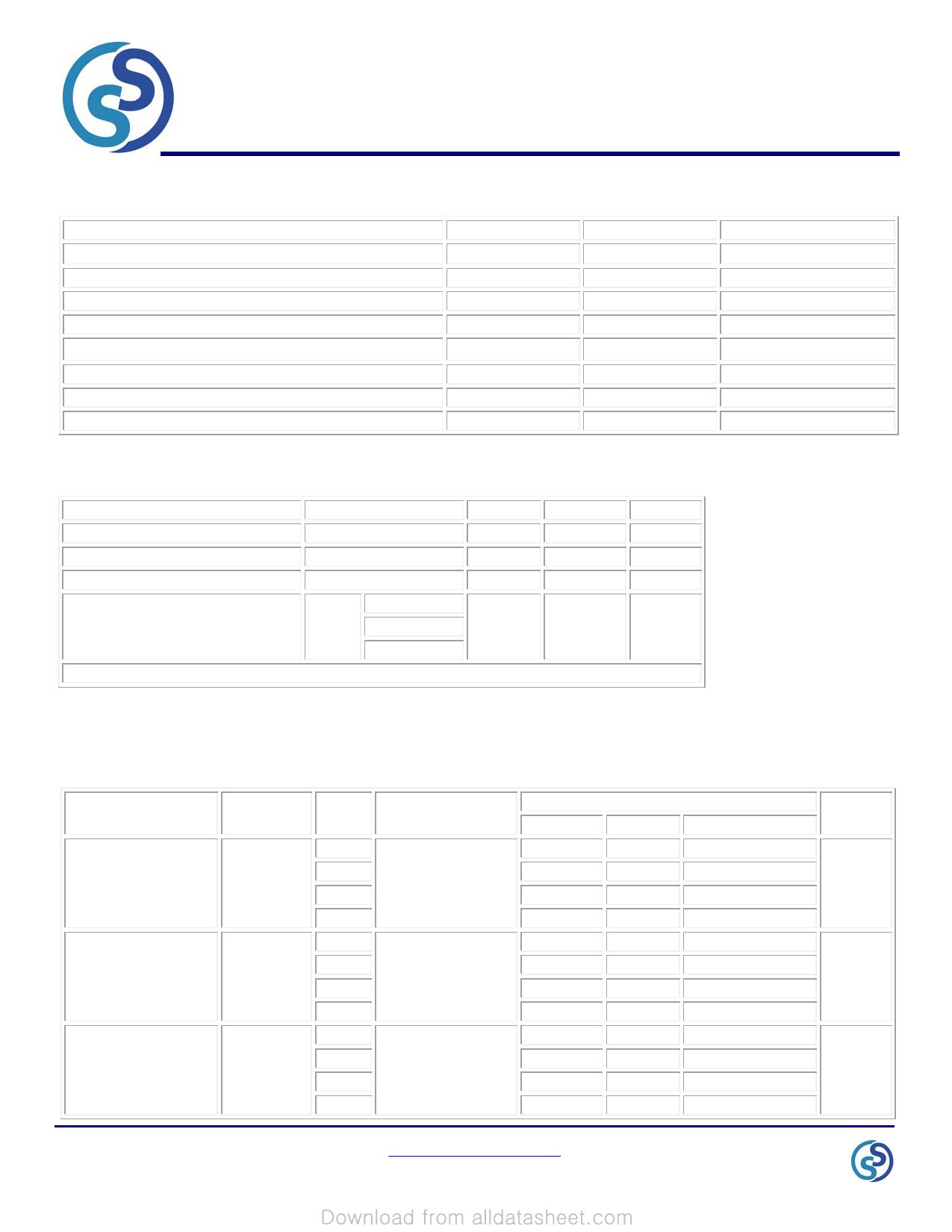
Absolute Maximum Ratings1
Rev 1.0
24/11/17
PARAMETER
SYMBOL
VALUE
UNIT
DC Supply Voltage (Referenced to GND)
VCC
-0.5 to +7.0
V
DC Input Voltage (Referenced to GND)
VIN
-0.5 to VCC +0.5
V
DC Output Voltage (Referenced to GND)
VOUT
-0.5 to VCC +0.5
V
DC Input Current
IIN
±20
mA
DC Output Current, per pad
IOUT
±25
mA
DC Supply Current, VCC or GND, per pad
Power Dissipation in Still Air2
ICC
±50
mA
PD
750
mW
Storage Temperature Range
TSTG
-65 to 150
°C
1. Operation above the absolute maximum rating may cause device failure. Operation at the absolute maximum ratings, for extended periods, may
reduce device reliability. 2. Measured in plastic DIP package, results in die form are dependent on die attach and assembly method.
Recommended Operating Conditions3 (Voltages Referenced to GND)
PARAMETER
SYMBOL
MIN
MAX UNITS
Supply Voltage
DC Input or Output Voltage
VCC
VIN ,VOUT
2
6
V
0
VCC
V
Operating Temperature Range
TJ
0
+85
°C
Input Rise or Fall Times
VCC = 2.0V
tr, tf VCC = 4.5V
-
No limit*
ns
VCC = 6.0V
* When VIN = 50% VCC, ICC > 1mA.
3. This device contains protection circuitry to guard against damage due to high static voltages or electric fields. However, precautions must be taken
to avoid applications of any voltage higher than maximum rated voltages to this high-impedance circuit. For proper operation, VIN and VOUT should be
constrained to the range GND ≤ (VIN or VOUT) ≤ VCC. Unused inputs must always be tied to an appropriate logic voltage level (e.g., either GND or VCC).
Unused outputs must be left open.
DC Electrical Characteristics (Voltages referenced to GND)
PARAMETER
SYMBOL VCC
CONDITIONS
25°C
LIMITS
85°C FULL RANGE4
UNITS
2.0V
1.50
1.50
1.50
Maximum Positive-
Going Input
Threshold Voltage
VT+ MAX
3.0V
4.5V
VOUT = 0.1V
│IOUT│≤ 20µA
2.15
3.15
2.15
3.15
2.15
3.15
V
6.0V
4.20
4.20
4.20
2.0V
1.0
0.95
0.95
Minimum Positive-
Going Input
Threshold Voltage
VT+ MIN
3.0V
4.5V
VOUT = 0.1V
│IOUT│≤ 20µA
1.5
2.3
1.45
2.25
1.45
2.25
V
6.0V
3.0
2.95
2.95
Maximum
2.0V
0.9
0.95
0.95
Negative-Going
Input Threshold
VT- MAX
3.0V
4.5V
VOUT = VCC -0.1V
│IOUT│≤ 20µA
1.4
2.0
1.45
2.05
1.45
2.05
V
Voltage
6.0V
2.6
2.65
2.65
Page 3 of 5
www.siliconsupplies.com
Share Link: 