MMFT107T1 查看數據表(PDF) - ON Semiconductor
零件编号
产品描述 (功能)
生产厂家
MMFT107T1 Datasheet PDF : 7 Pages
| |||
MMFT107T1
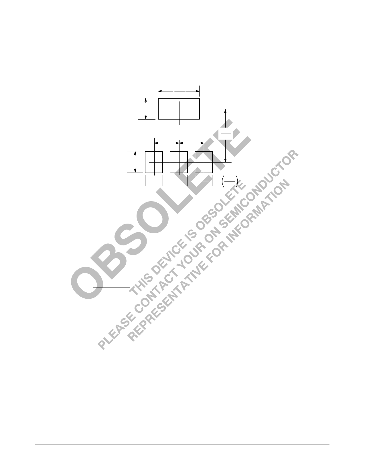
INFORMATION FOR USING THE SOT-223 SURFACE MOUNT PACKAGE
MINIMUM RECOMMENDED FOOTPRINT FOR SURFACE MOUNTED APPLICATIONS
Surface mount board layout is a critical portion of the
total design. The footprint for the semiconductor packages
must be the correct size to insure proper solder connection
interface between the board and the package. With the
correct pad geometry, the packages will self align when
subjected to a solder reflow process.
0.15
3.8
0.079
2.0
0.079
2.0
0.091
2.3
0.091
2.3
0.248
6.3
0.059
1.5
0.059
1.5
0.059
1.5
inches
mm
SOT-223 POWER DISSIPATION
The power dissipation of the SOT-223 is a function of the
pad size. This can vary from the minimum pad size for
soldering to a pad size given for maximum power
dissipation. Power dissipation for a surface mount device is
determined by TJ(max), the maximum rated junction
temperature of the die, RθJA, the thermal resistance from
the device junction to ambient, and the operating
temperature, TA. Using the values provided on the data
sheet for the SOT-223 package, PD can be calculated as
follows:
PD =
TJ(max) − TA
RθJA
The values for the equation are found in the maximum
ratings table on the data sheet. Substituting these values
into the equation for an ambient temperature TA of 25°C,
one can calculate the power dissipation of the device which
in this case is 0.8 watts.
PD = 150°C − 25°C = 0.8 watts
156°C/W
The 156°C/W for the SOT-223 package assumes the use
of the recommended footprint on a glass epoxy printed
circuit board to achieve a power dissipation of 0.8 watts.
There are other alternatives to achieving higher power
dissipation from the SOT-223 package. One is to increase
the area of the collector pad. By increasing the area of the
collector pad, the power dissipation can be increased.
Although the power dissipation can almost be doubled with
this method, area is taken up on the printed circuit board
which can defeat the purpose of using surface mount
technology. A graph of RθJA versus collector pad area is
shown in Figure 9.
http://onsemi.com
4
Share Link: 