MC12429FN 查看數據表(PDF) - Motorola => Freescale
零件编号
产品描述 (功能)
生产厂家
MC12429FN Datasheet PDF : 10 Pages
| |||
MC12429
from a 16.666MHz reference the following M and N values
would be used:
FOUT = 16.666 ÷ 8 x M ÷ N = 2.083333 x M ÷ N
Let N = 4, M = 133.3333 ÷ 2.083333 x 4 = 256
The value for M falls within the constraints set for PLL
stability, therefore N[1:0] = 01 and M[8:0} = 10000000. If the
value for M fell outside of the valid range a different N value
would be selected to try to move M in the appropriate
direction.
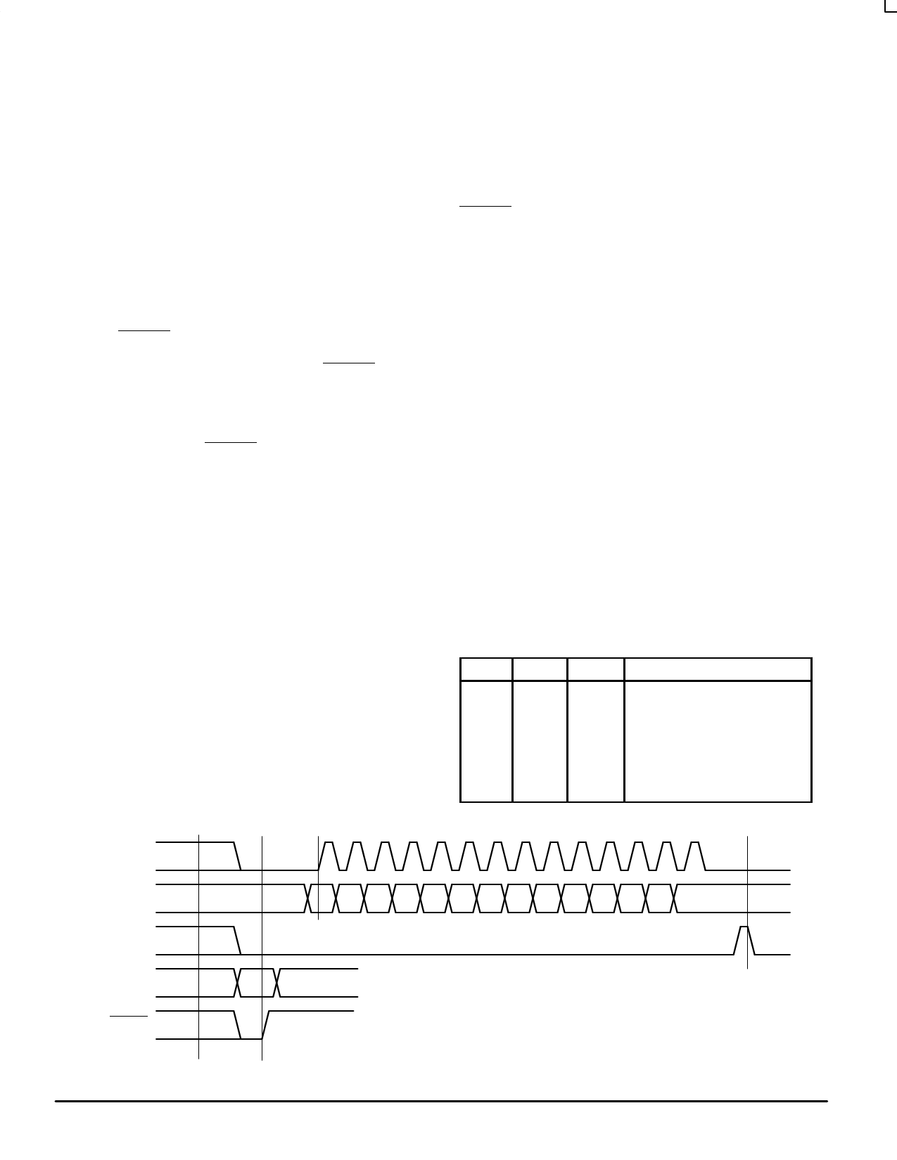
The M and N counters can be loaded either through a
parallel or serial interface. The parallel interface is controlled
via the P_LOAD signal such that a LOW to HIGH transition
will latch the information present on the M[8:0] and N[1:0]
inputs into the M and N counters. When the P_LOAD signal is
LOW the input latches will be transparent and any changes
on the M[8:0] and N[1:0] inputs will affect the FOUT output
pair. To use the serial port the S_CLOCK signal samples the
information on the S_DATA line and loads it into a 14 bit shift
register. Note that the P_LOAD signal must be HIGH for the
serial load operation to function. The Test register is loaded
with the first three bits, the N register with the next two and
the M register with the final eight bits of the data streeam on
the S_DATA input. For each register the most significant bit is
loaded first (T2, N1 and M8). A pulse on the S_LOAD pin
after the shift register is fully loaded will transfer the divide
values into the counters. The HIGH to LOW transition on the
S_LOAD input will latch the new divide values into the
counters. Figure 3 illustrates the timing diagram for both a
parallel and a serial load of the MC12429 synthesizer.
M[8:0] and N[1:0] are normally specified once at power–up
through the parallel interface, and then possibly again
through the serial interface. This approach allows the
application to come up at one frequency and then change or
fine–tune the clock as the ability to control the serial interface
becomes available. To minimize transients in the frequency
domain, the output should be varied in the smallest step size
possible. The bandwidth of the PLL is such that frequency
stepping in 1MHz steps at the maximum S_CLOCK
frequency or less will cause smooth, controlled slewing of the
output frequency.
The TEST output provides visibility for one of the several
internal nodes as determined by the T[2:0] bits in the serial
configuration stream. It is not configurable through the
parallel interface. Although it is possible to select the node
that represents FOUT, the CMOS output may not be able to
toggle fast enough for some of the higher output frequencies.
The T2, T1 and T0 control bits are preset to ‘000’ when
P_LOAD is LOW so that the PECL FOUT outputs are as
jitter–free as possible. Any active signal on the TEST output
pin will have detrimental affects on the jitter of the PECL
output pair. In normal operations, jitter specifications are only
guaranteed if the TEST output is static. The serial
configuration port can be used to select one of the alternate
functions for this pin.
Most of the signals available on the TEST output pin are
useful only for performance verification of the MC12429
itself. However the PLL bypass mode may be of interest at
the board level for functional debug. When T[2:0] is set to 110
the MC12429 is placed in PLL bypass mode. In this mode the
S_CLOCK input is fed directly into the M and N dividers. The
N divider drives the FOUT differential pair and the M counter
drives the TEST output pin. In this mode the S_CLOCK input
could be used for low speed board level functional test or
debug. Bypassing the PLL and driving FOUT directly gives
the user more control on the test clocks sent through the
clock tree. Figure 4 shows the functional setup of the PLL
bypass mode. Because the S_CLOCK is a CMOS level the
input frequency is limited to 250MHz or less. This means the
fastest the FOUT pin can be toggled via the S_CLOCK is
125MHz as the minimum divide ratio of the N counter is 2.
Note that the M counter output on the TEST output will not be
a 50% duty cycle due to the way the divider is implemented.
T2
T1
0
0
0
0
0
1
0
1
1
0
1
0
1
1
1
1
T0
TEST (Pin 20)
0
SHIFT REGISTER OUT
1
HIGH
0
FREF
1
M COUNTER OUT
0
FOUT
1
LOW
0
PLL BYPASS
1
FOUT/4
S_CLOCK
S_DATA
S_LOAD
M[8:0]
N[1:0]
P_LOAD
T2 T1 T0 N1 N0 M8 M7 M6 M5 M4 M3 M2 M1 M0
First
Last
Bit
Bit
M, N
Figure 3. Timing Diagram
MOTOROLA
4
TIMING SOLUTIONS
BR1333 — Rev 6
Share Link: 