MC12429FN 查看數據表(PDF) - Motorola => Freescale
零件编号
产品描述 (功能)
生产厂家
MC12429FN Datasheet PDF : 10 Pages
| |||
MC12429
Power Supply Filtering
The MC12429 is a mixed analog/digital product and as
such it exhibits some sensitivities that would not necessarily
be seen on a fully digital product. Analog circuitry is naturally
susceptible to random noise, especially if this noise is seen
on the power supply pins. The MC12429 provides separate
power supplies for the digital ciruitry (VCC) and the internal
PLL (PLL_VCC) of the device. The purpose of this design
technique is to try and isolate the high switching noise digital
outputs from the relatively sensitive internal analog
phase–locked loop. In a controlled environment such as an
evaluation board this level of isolation is sufficient. However,
in a digital system environment where it is more difficult to
minimize noise on the power supplies a second level of
isolation may be required. The simplest form of isolation is a
power supply filter on the PLL_VCC pin for the MC12429.
Figure 5 illustrates a typical power supply filter scheme.
The MC12429 is most susceptible to noise with spectral
content in the 1KHz to 1MHz range. Therefore the filter
should be designed to target this range. The key parameter
that needs to be met in the final filter design is the DC voltage
drop that will be seen between the VCC supply and the
PLL_VCC pin of the MC12429. From the data sheet the
IPLL_VCC current (the current sourced through the PLL_VCC
pin) is typically 15mA (20mA maximum), assuming that a
minimum of 3.0V must be maintained on the PLL_VCC pin
very little DC voltage drop can be tolerated when a 3.3V VCC
supply is used. The resistor shown in Figure 5 must have a
resistance of 10–15Ω to meet the voltage drop criteria. The
RC filter pictured will provide a broadband filter with
approximately 100:1 attenuation for noise whose spectral
content is above 20KHz. As the noise frequency crosses the
series resonant point of an individual capacitor it’s overall
impedance begins to look inductive and thus increases with
increasing frequency. The parallel capacitor combination
shown ensures that a low impedance path to ground exists
for frequencies well above the bandwidth of the PLL.
3.3V or
5.0V
3.3V or
5.0V
RS=10–15Ω
PLL_VCC
MC12429
22µF
0.01µF
VCC
0.01µF
L=1000µH
R=15Ω
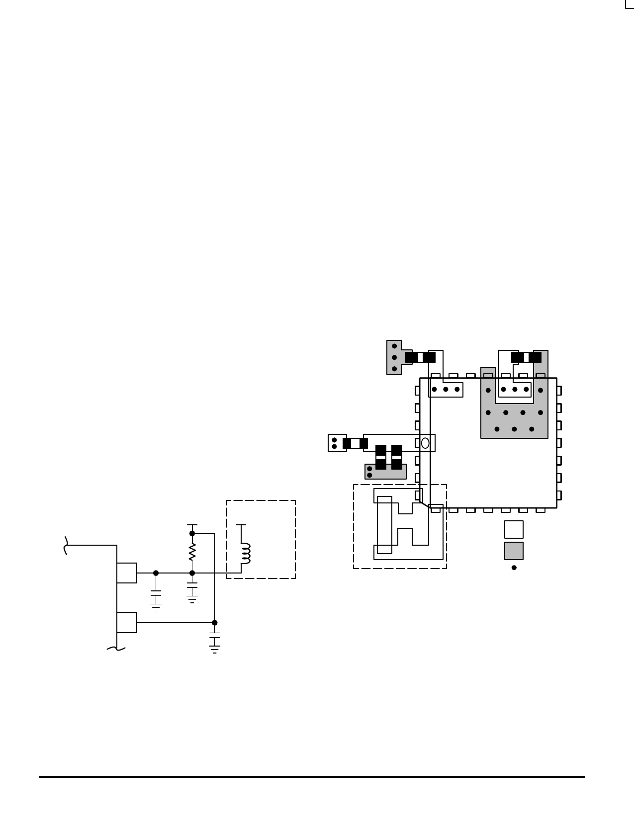
Figure 5. Power Supply Filter
A higher level of attenuation can be acheived by replacing
the resistor with an appropriate valued inductor. Figure 5
shows a 1000µH choke, this value choke will show a
significant impedance at 10KHz frequencies and above.
Because of the current draw and the voltage that must be
maintained on the PLL_VCC pin a low DC resistance
inductor is required (less than 15Ω). Generally the
resistor/capacitor filter will be cheaper, easier to implement
and provide an adequate level of supply filtering.
The MC12429 provides sub–nanosecond output edge
rates and thus a good power supply bypassing scheme is a
must. Figure 6 shows a representaive board layout for the
MC12429. There exists many different potential board
layouts and the one pictured is but one. The important aspect
of the layout in Figure 6 is the low impedance connections
between VCC and GND for the bypass capacitors.
Combining good quality general purpose chip capacitors with
good PCB layout techniques will produce effective capacitor
resonances at frequencies adequate to supply the
instantaneous switching current for the 12429 outputs. It is
imperative that low inductance chip capacitors are used; it is
equally important that the board layout does not introduce
back all of the inductance saved by using the leadless
capacitors. Thin interconnect traces between the capacitor
and the power plane should be avoided and multiple large
vias should be used to tie the capacitors to the buried power
planes. Fat interconnect and large vias will help to minimize
layout induced inductance and thus maximize the series
resonant point of the bypass capacitors.
ÉÉÉÉC1 ÉÉÉÉÉÉÉÉÉÉÉÉ ÉÉÉÉÉÉÉÉCÉÉÉÉ1
ÉÉÉÉR1
1
C3
C2
Xtal
R1 = 10–15Ω
C1 = 0.01µF
C2 = 22µF
C3 = 0.1µF
ÉÉÉÉ= VCC
= GND
= Via
Figure 6. PCB Board Layout for MC12429
Note the dotted lines circling the crystal oscillator
connection to the device. The oscillator is a series resonant
circuit and the voltage amplitude across the crystal is
relatively small. It is imperative that no actively switching
signals cross under the crystal as crosstalk energy coupled
to these lines could significantly impact the jitter of the device.
Special attention should be paid to the layout of the crystal to
ensure a stable, jitter free interface between the crystal and
the on–board oscillator. Note the provisions for placing a
resistor across the crystal oscillator terminals as discussed in
the crystal oscillator section of this data sheet.
Although the MC12429 has several design features to
minimize the susceptibility to power supply noise (isolated
power and grounds and fully differential PLL) there still may
TIMING SOLUTIONS
7
BR1333 — Rev 6
MOTOROLA
Share Link: 