ADG1411 وں¥çœ‹و•¸و“ڑè،¨ï¼ˆPDF) - Analog Devices
零ن»¶ç¼–هڈ·
ن؛§ه“پوڈڈè؟° (هٹں能)
ç”ںن؛§هژ‚ه®¶
ADG1411 Datasheet PDF : 16 Pages
| |||
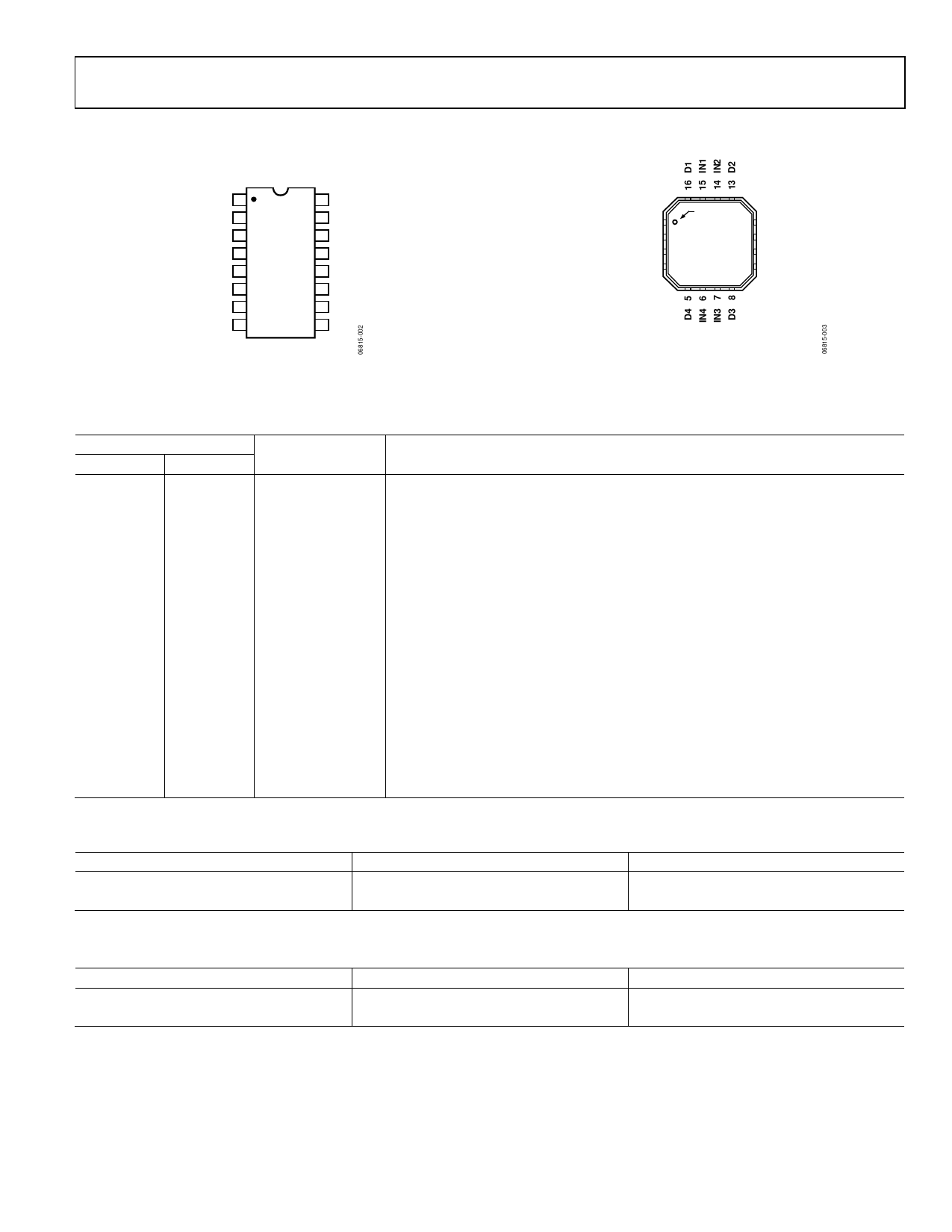
PIN CONFIGURATIONS AND FUNCTION DESCRIPTIONS
ADG1411/ADG1412/ADG1413
IN1 1
16 IN2
D1 2
15 D2
S1 3 ADG1411/ 14 S2
ADG1412/
VSS 4 ADG1413 13 VDD
GND 5
12 NC
TOP VIEW
S4 6 (Not to Scale) 11 S3
D4 7
10 D3
IN4 8
9 IN3
NC = NO CONNECT
Figure 2. TSSOP Pin Configuration
S1 1
VSS 2
GND 3
S4 4
PIN 1
INDICATOR
ADG1411/
ADG1412/
ADG1413
TOP VIEW
(Not to Scale)
12 S2
11 VDD
10 NC
9 S3
NOTES
1. EXPOSED PAD TIED TO SUBSTRATE, VSS.
2. NC = NO CONNECT.
Figure 3. LFCSP Pin Configuration
Table 5. Pin Function Descriptions
Pin No.
TSSOP
LFCSP
Mnemonic
1
15
IN1
2
16
D1
3
1
S1
4
2
VSS
5
3
GND
6
4
S4
7
5
D4
8
6
IN4
9
7
IN3
10
8
D3
11
9
S3
12
10
NC
13
11
VDD
14
12
S2
15
13
D2
16
14
IN2
N/A1
0
EP
1 N/A means not applicable.
Description
Logic Control Input.
Drain Terminal. This pin can be an input or output.
Source Terminal. This pin can be an input or output.
Most Negative Power Supply Potential.
Ground (0 V) Reference.
Source Terminal. This pin can be an input or output.
Drain Terminal. This pin can be an input or output.
Logic Control Input.
Logic Control Input.
Drain Terminal. This pin can be an input or output.
Source Terminal. This pin can be an input or output.
No Connection.
Most Positive Power Supply Potential.
Source Terminal. This pin can be an input or output.
Drain Terminal. This pin can be an input or output.
Logic Control Input.
Exposed Pad. Tie the exposed pad to the substrate, VSS.
Table 6. ADG1411/ADG1412 Truth Table
ADG1411 INx
0
1
ADG1412 INx
1
0
Switch Condition
On
Off
Table 7. ADG1413 Truth Table
ADG1413 INx
0
1
S1, S4
Off
On
S2, S3
On
Off
Rev. B | Page 7 of 16
Share Link: 