EN5312QI 查看數據表(PDF) - Enpirion, Inc.
零件编号
产品描述 (功能)
生产厂家
EN5312QI Datasheet PDF : 16 Pages
| |||
March 2007
LAYOUT CONSIDERATIONS*
EN5312QI
*Optimized PCB Layout file downloadable from the Enpirion Website to assure first pass design success.
Recommendation 1: Input and output filter capacitors should be placed as close to the EN5312QI
package as possible to reduce EMI from input and output loop AC currents. This reduces the
physical area of the Input and Output AC current loops.
Recommendation 2: DO NOT connect GND pins 3 and 4 together. Pin 3 should be used for the
Input capacitor local ground and pin 4 should be used for the output capacitor ground. The ground
pad for the input and output filter capacitors should be isolated ground islands and should be
connected to system ground as indicated in recommendation 3 and recommendation 5.
Recommendation 3: Multiple small vias (0.25mm after copper plating) should be used to connect
ground terminals of the Input capacitor and the output capacitor to the system ground plane. This
provides a low inductance path for the high-frequency AC currents, thereby reducing ripple and
suppressing EMI (see Fig. 5, Fig. 6, and Fig. 7).
Recommendation 4: The large thermal pad underneath the component must be connected to the
system ground plane through as many thermal vias as possible. The vias should use 0.33mm drill
size with minimum one ounce copper plating (0.035mm plating thickness). This provides the path for
heat dissipation from the converter.
Recommendation 5: The system ground plane referred to in recommendations 3 and 4 should be
the first layer immediately below the surface layer (PCB layer 2). This ground plane should be
continuous and un-interrupted below the converter and the input and output capacitors that carry
large AC currents. If it is not possible to make PCB layer 2 a continuous ground plane, an
uninterrupted ground “island” should be created on PCB layer 2 immediately underneath the
EN5312QI and its input and output capacitors. The vias that connect the input and output capacitor
grounds, and the thermal pad to the ground island, should continue through to the PCB GND layer as
well.
Recommendation 6: As with any switch-mode DC/DC converter, do not run sensitive signal or
control lines underneath the converter package.
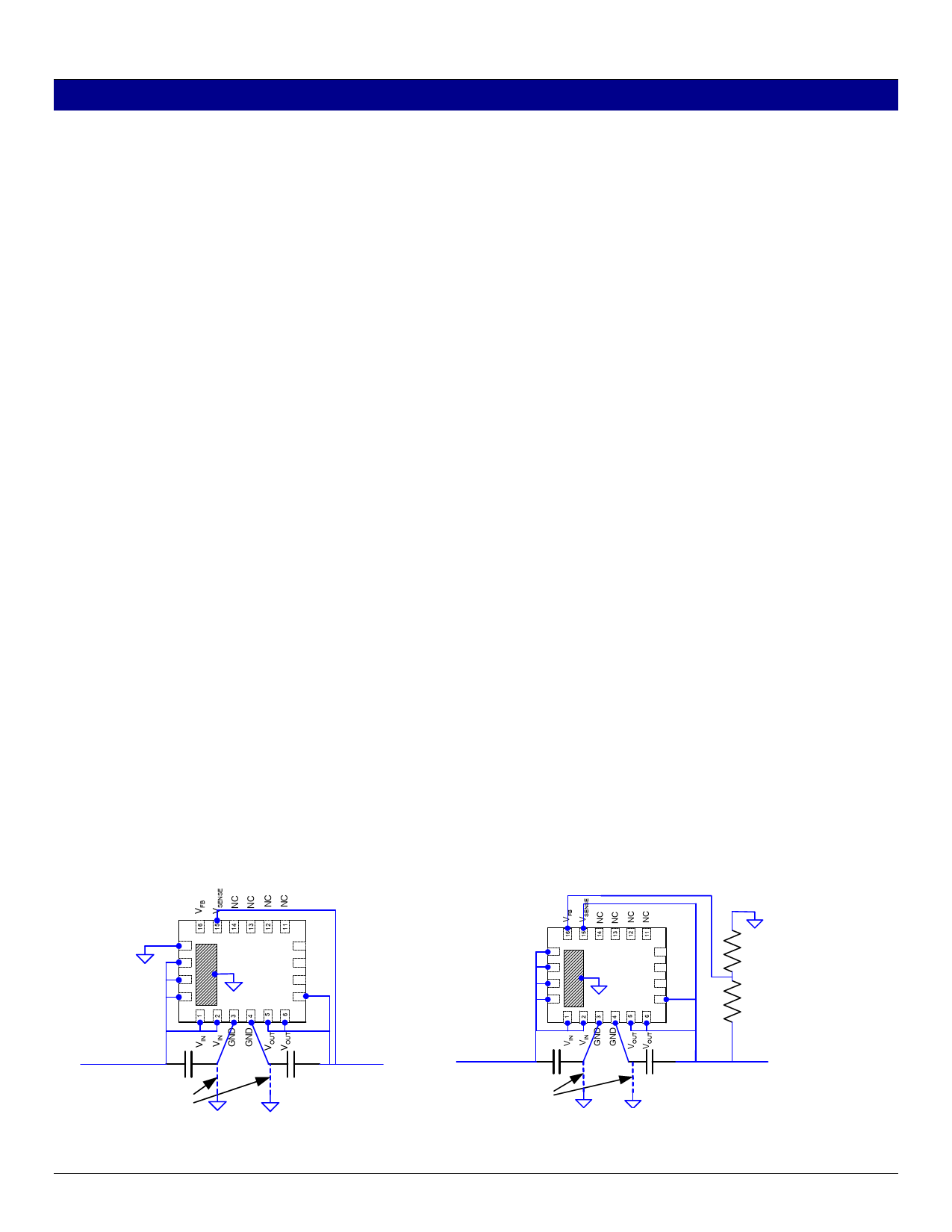
Figure 5 shows an example schematic for the EN5312QI using the internal voltage select. In this
example, the device is set to a VOUT of 1.5V (VS2=0, VS1=1, VS0=1).
VS2
17
VS1 18
VS0
19
ENABLE 20
10 NC
9 NC
8 NC
7 VOUT
VS2 17
VS1 18
VS0
19
ENABLE 20
10 NC
9 NC
8 NC
7 VOUT
Rb=60K
Ra=200K
VIN
4.7uF
(see layout recommendation 3)
10µF
VOUT
VIN
4.7uF
(see layout recommendation 3)
10µF
VOUT
Figure 5. Example application, Vout=1.5V.
©Enpirion 2007 all rights reserved, E&OE
Figure 6. Example Application, external divider, Vout = 2.6V.
10
www.enpirion.com
Share Link: 