EN5312QI 查看數據表(PDF) - Enpirion, Inc.
零件编号
产品描述 (功能)
生产厂家
EN5312QI Datasheet PDF : 16 Pages
| |||
March 2007
EN5312QI
Figure 6 shows an example schematic using an external voltage divider. VS0=VS1=VS2= “1”. The
resistor values are chosen to give an output voltage of 2.6V.
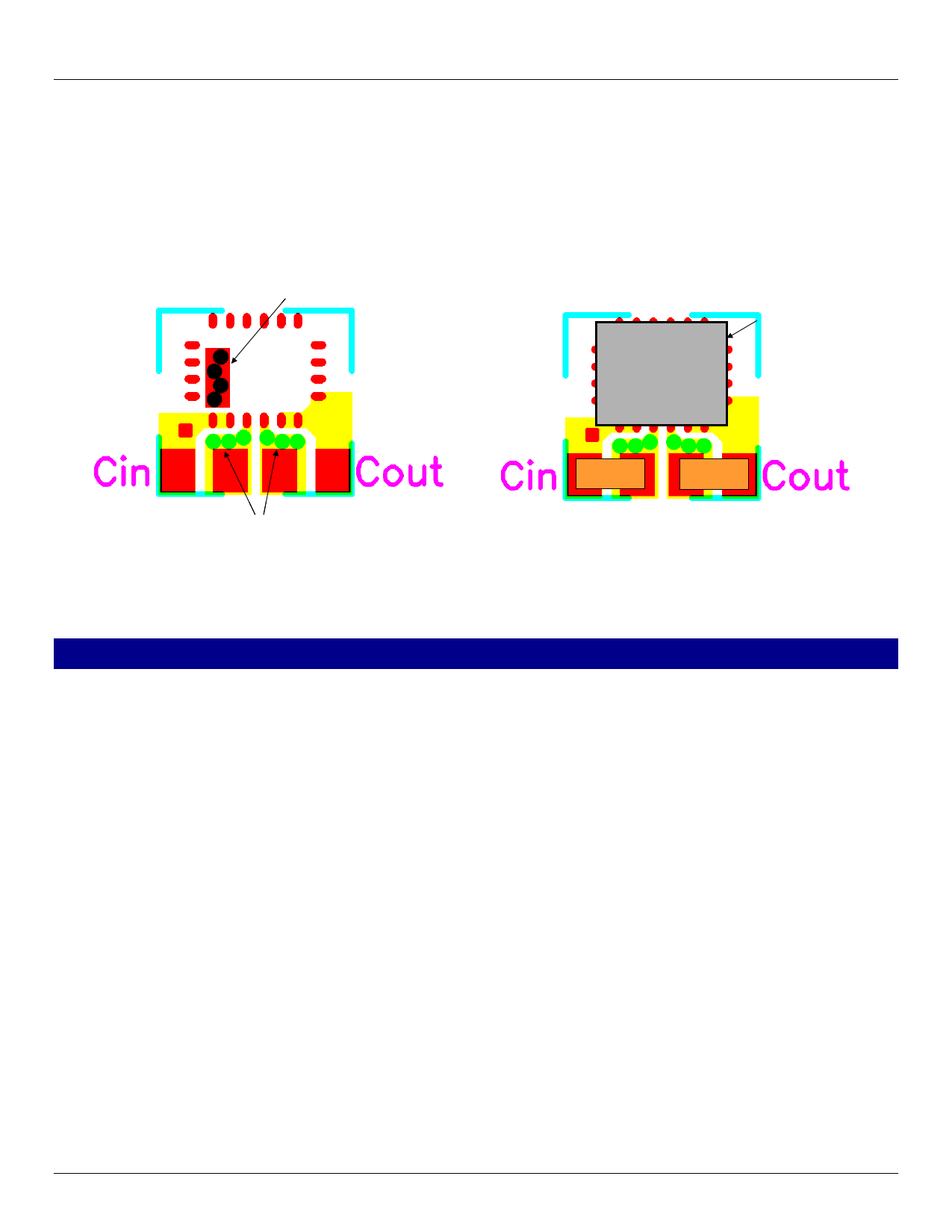
Figure 7 shows an example board layout. The left side of the figure demonstrates construction of the
PCB top layer. Note the placement of the vias from the input and output filter capacitor grounds, and
the thermal pad, to the PCB ground on layer 2 (1st layer below PCB surface). The right side of the
figure shows the layout with the components populated. Note the placement of the vias per
recommendation 3.
Thermal Vias to Ground Plane
Package
Outline
Vias to Ground Plane
CIN
COUT
Figure 7. Example layout showing PCB top layer, as well as demonstrating use of vias from input, output filter
capacitor local grounds, and thermal pad, to PCB system ground.
Design Considerations for Lead-Frame Based Modules
Exposed Metal on Bottom Of Package
Enpirion has developed a break-through in package technology that utilizes the lead frame as part of
the electrical circuit. The lead frame offers many advantages in thermal performance, in reduced
electrical lead resistance, and in overall foot print. However, it does require some special
considerations.
As part of the package assembly process, lead frame construction requires that for mechanical
support, some of the lead-frame cantilevers be exposed at the point where wire-bond or internal
passives are attached. This results in several small pads being exposed on the bottom of the
package.
Only the large thermal pad and the perimeter pin pads are to be mechanically or electrically
connected to the PC board. The PCB top layer under the EN5312QI should be clear of any metal
except for the large thermal pad. The “grayed-out” area in Figure 8 represents the area that should
be clear of any metal (traces, vias, or planes), on the top layer of the PCB.
NOTE: Clearance between the various exposed metal pads, the thermal ground pad, and the
perimeter pins, meets or exceeds JEDEC requirements for lead frame package construction (JEDEC
MO-220, Issue J, Date May 2005). The separation between the large thermal pad and the nearest
adjacent metal pad or pin is a minimum of 0.20mm, including tolerances. This is shown in Figure 9.
©Enpirion 2007 all rights reserved, E&OE
11
www.enpirion.com
Share Link: 