LTC699IS8 查看數據表(PDF) - Linear Technology
零件编号
产品描述 (功能)
生产厂家
LTC699IS8 Datasheet PDF : 4 Pages
| |||
LTC699
PI FU CTIO S
VCC: +5V supply input. The VCC pin should be bypassed
with a 0.1µF capacitor.
GND: Ground pin.
RESET: Open drain output for µP reset control. When VCC
falls below the reset voltage threshold (4.65V typically),
RESET goes active low. After VCC returns to 5V, the reset
pulse generator forces RESET to remain active low for a
minimum of 140ms . When the watchdog timer is enabled
but not serviced prior to the time-out period, the reset
pulse generator also forces RESET to active low for a mini-
mum of 140ms for every time-out period (see Figure 2).
WDI: Watchdog Input, WDI, is a three level input. Driving
WDI either high or low for longer than the watchdog time-
out period forces RESET low. Floating WDI disables the
Watchdog Timer. The timer resets itself with each transition
of the Watchdog Input (see Figure 2).
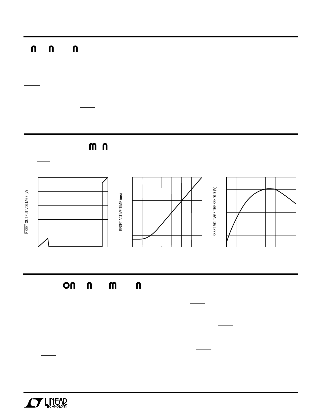
TYPICAL PERFOR A CE CHARACTERISTICS
RESET Output Voltage vs
Supply Voltage
5
TA = 25°C
EXTERNAL PULLUP = 10µA
4
3
2
1
0
0
1
2
3
4
5
SUPPLY VOLTAGE (V)
LTC699 G01
Reset Active Time vs
Temperature
232
VCC = 5V
224
216
208
200
192
184
–50 –25
0 25 50 75
TEMPERATURE (°C)
100 125
LTC699 G02
Reset Voltage Threshold vs
Temperature
4.66
4.65
4.64
4.63
4.62
4.61
4.60
–50 –25
0 25 50 75
TEMPERATURE (°C)
100 125
LTC699 G03
APPLICATI S I FOR ATIO
Microprocessor Reset
The LTC699 uses a bandgap voltage reference and a
precision voltage comparator C1 to monitor the 5V supply
input VCC (see BLOCK DIAGRAM). When VCC falls below
the reset voltage threshold, the RESET output is forced to
active low state. The reset voltage threshold accounts for
a 5% variation on VCC, so the RESET output becomes
active low when VCC falls below 4.65V typical. On power-
up, the RESET signal is held active low for a minimum of
140ms after reset voltage threshold is reached to allow the
power supply and microprocessor to stabilize. On power-
down, the RESET signal remains active low even with VCC
as low as 1V. This capability helps hold the microproces-
sor in stable shutdown condition. Figure 1 shows the
timing diagram of the RESET signal.
The precision voltage comparator, C1, typically has 40mV
of hysteresis which ensures that glitches at VCC pin do not
activate the RESET output. Response time is typically
10µs. To help prevent mistriggering due to transient loads,
VCC pin should be bypassed with a 0.1µF capacitor with the
leads trimmed as short as possible.
Information furnished by Linear Technology Corporation is believed to be accurate and reliable.
However, no responsibility is assumed for its use. Linear Technology Corporation makes no represen-
tation that the interconnection of circuits as described herein will not infringe on existing patent rights.
3
Share Link: 