SL1710 查看數據表(PDF) - Zarlink Semiconductor Inc
零件编号
产品描述 (功能)
生产厂家
SL1710 Datasheet PDF : 12 Pages
| |||
SL1710 Preliminary Information
I & Q OUTPUTS
The I and Q output stages of the SL1710 are sensitive to the
loads connected to them. To avoid degrading the output
signals resistive loads connected to these pins should always
be 1KΩ or greater with a parallel capacitance of 15pF or less
For evaluation purposes this makes the output unsuitable
for connection to test equipment via normal coaxial cables. To
alleviate this problem the application board is fitted with
emitter follower buffer amplifiers which allow the connection of
loads as low as 50Ω via coaxial cables without loading the
output stages of the SL1710. These buffer amplifiers can be
either connected in circuit, or bypassed by changing the
position of Links 1 and 2.
This technique may be used in a real application where the
SL1710 is used to drive and ADC via an anti-alias filter. Great
care must be taken to ensure that the loading conditions
stated above are not exceeded when designing the anti-alias
filter section. Use of an emitter follower buffer is the easiest
way to alleviate this constraint.
With the AGC voltage adjusted to 2.5 Volts apply an input
signal to the IF IN (pin 5) and monitor the Base Band output
level at the I and Q outputs. Adjust the RF input level until an
output level of 760mV pk-pk is achieved. For best
performance this level should not exceeded.
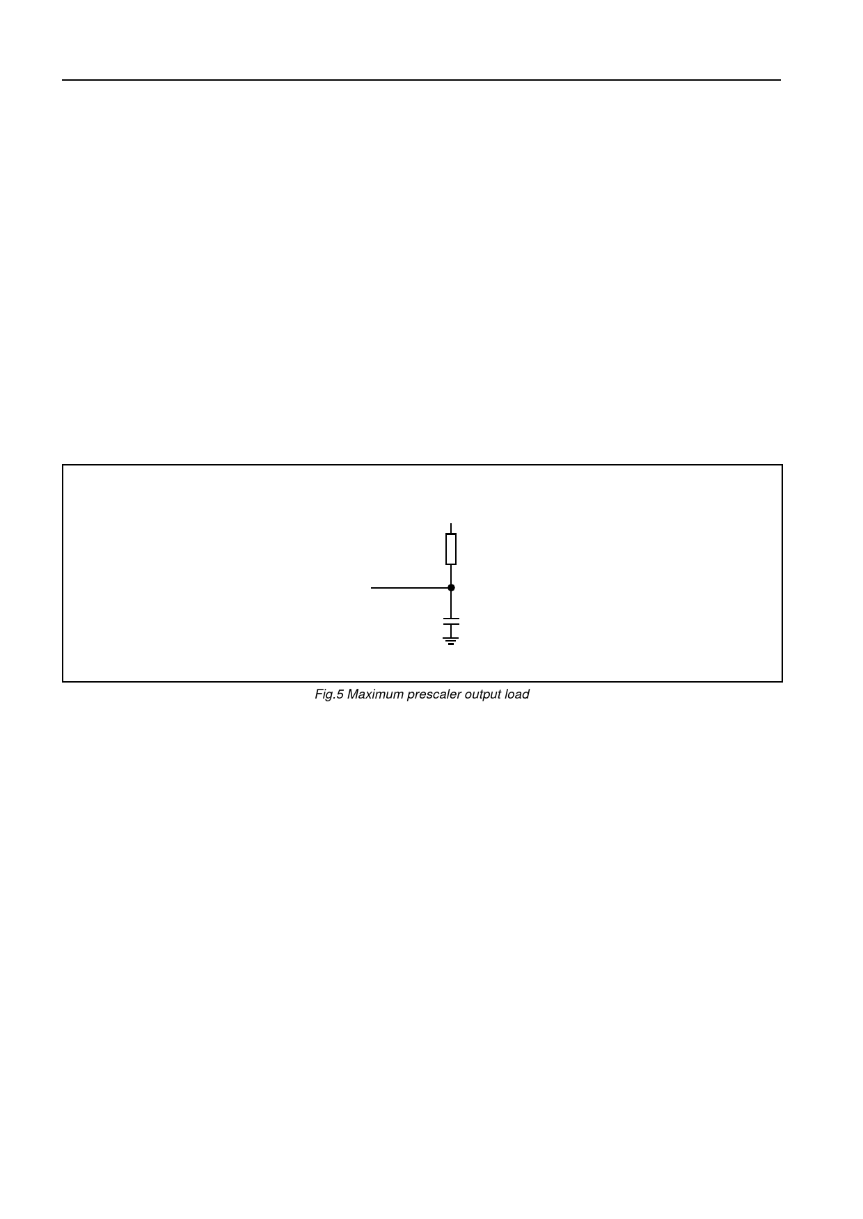
PRESCALER
OUTPUT
Vcc 2
2K
15pF
Fig.5 Maximum prescaler output load
6
Share Link: 