MAX44260 查看數據表(PDF) - Maxim Integrated
零件编号
产品描述 (功能)
生产厂家
MAX44260 Datasheet PDF : 14 Pages
| |||
MAX44259/MAX44260/
MAX44261/MAX44263
1.8V, 15MHz Low-Offset,
Low-Power, Rail-to-Rail I/O Op Amps
Absolute Maximum Ratings
IN+, IN-, OUT................................. (VSS - 0.3V) to (VDD + 0.3V)
VDD to VSS...............................................................-0.3V to +6V
SHDN, CAL..............................................................-0.3V to +6V
Output to Short-Circuit Ground Duration............................... 10s
Continuous Input Current into Any Pin............................. Q20mA
Continuous Power Dissipation (TA = +70NC)
SC70 (derate 3.1mW/NC above +70NC).......................245mW
SOT23 (derate 3.9mW/NC above +70NC)..................312.6mW
6-Pin Thin µDFN (Ultra-Thin LGA)
(derate 2.1mW/NC above +70NC)..............................110.2mW
Operating Temperature Range......................... -40NC to +125NC
Junction Temperature......................................................+150NC
Lead Temperature (soldering, 10s).................................+300NC
Soldering Temperature (reflow).......................................+260NC
Stresses beyond those listed under “Absolute Maximum Ratings” may cause permanent damage to the device. These are stress ratings only, and functional operation
of the device at these or any other conditions beyond those indicated in the operational sections of the specifications is not implied. Exposure to absolute maximum
rating conditions for extended periods may affect device reliability.
Package Thermal Characteristics (Note 1)
SC70
Junction-to-Ambient Thermal Resistance (BJA)..... 326.5NC/W
Junction-to-Case Thermal Resistance (BJC)..............115NC/W
SOT23
Junction-to-Ambient Thermal Resistance (BJA)..... 255.9NC/W
Junction-to-Case Thermal Resistance (BJC)................81NC/W
Thin µDFN (Ultra-Thin LGA)
Junction-to-Ambient Thermal Resistance (BJA)........ 470NC/W
Note 1: Package thermal resistances were obtained using the method described in JEDEC specification JESD51-7, using a four-layer
board. For detailed information on package thermal considerations, refer to www.maximintegrated.com/thermal-tutorial.
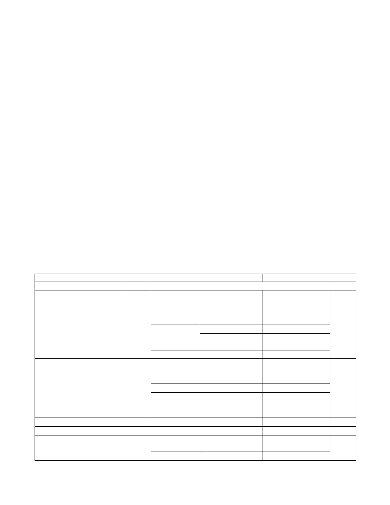
Electrical Characteristics
(VDD = 3.3V, VSS = 0V, VIN+ = VIN- = VDD/2, RL = 10kI to VDD/2, VCAL = VSHDN = VDD, TA = -40NC to +125NC. Typical values are
at TA = +25NC, unless otherwise noted.) (Note 2)
PARAMETER
DC CHARACTERISTICS
Input Voltage Range
SYMBOL
CONDITIONS
VIN+ VIN- Guaranteed by CMRR test
MIN TYP MAX UNITS
-0.1
VDD
+ 0.1
V
Input Offset Voltage (Note 3)
Input Offset Voltage Drift
(Note 3)
VOS
VOS - TC
TA = +25NC
TA = -40°C to +125°C after calibration
TA = -40°C to
+125°C
MAX44260/MAX44261
MAX44259/MAX44263
MAX44260/MAX44261
MAX44259/MAX44263
10
50
100
FV
500
800
0.8
5
FV/NC
1
8
TA = +25NC
MAX44259/
MAX44260/MAX44261
0.01 0.5
MAX44263
0.01 0.5
Input Bias Current (Note 3)
IB
TA = -40NC to +85NC
10
pA
TA = -40NC to
MAX44259/
MAX44260/MAX44261
100
+125NC
MAX44263
160
Input Capacitance
CIN
0.4
pF
Common-Mode Rejection Ratio
CMRR VCM = -0.1V to (VDD + 0.1V)
75
90
dB
Input Resistance
Common mode
RIN
VCM = -0.1V to
(VDD + 0.1V)
Differential mode
1011
Ω
1012
www.maximintegrated.com
Maxim Integrated │ 2
Share Link: 