LTC2858CMS8-2 查看數據表(PDF) - Analog Devices
零件编号
产品描述 (功能)
生产厂家
LTC2858CMS8-2 Datasheet PDF : 20 Pages
| |||

LTC2856-1/LTC2856-2
LTC2857-1/LTC2857-2
LTC2858-1/LTC2858-2
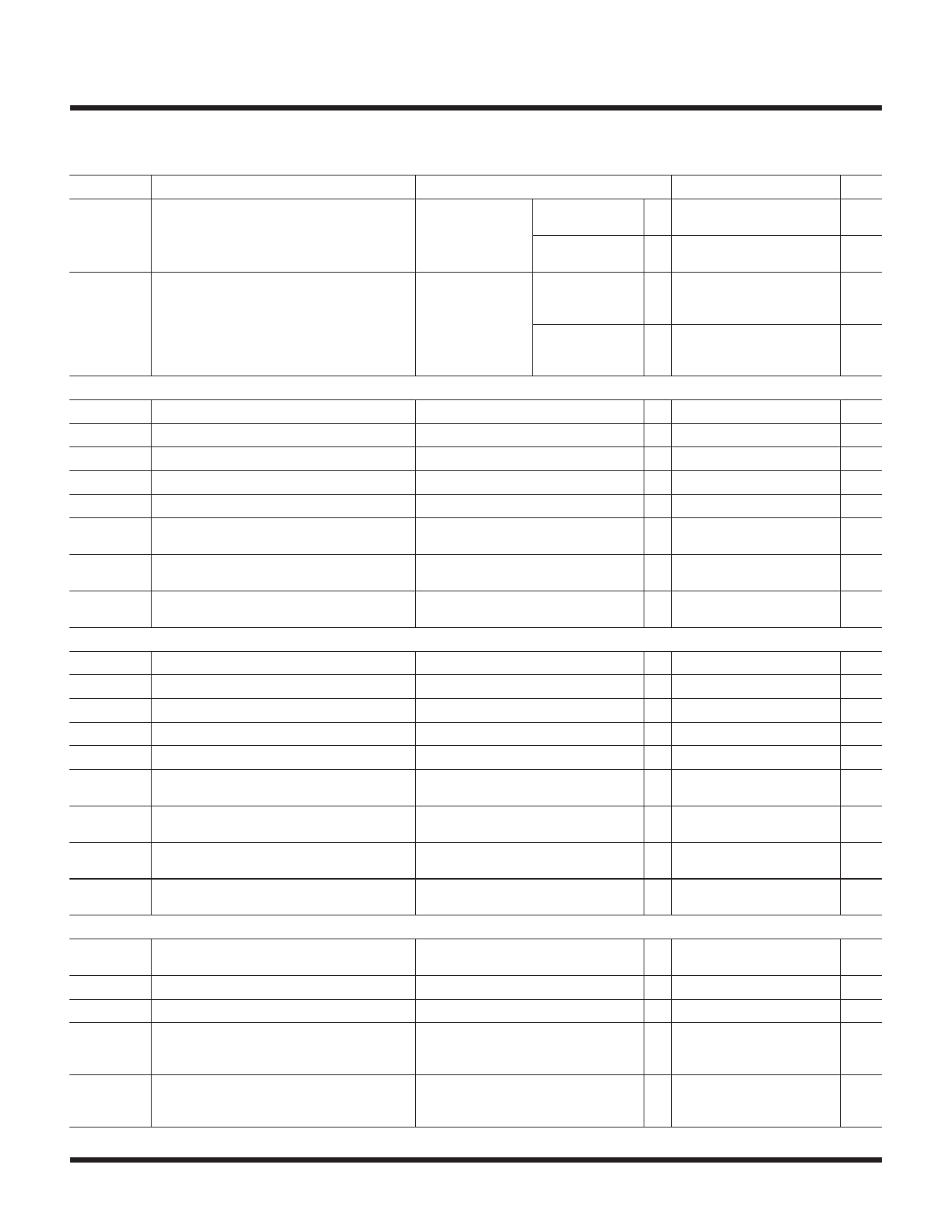
SWITCHING CHARACTERISTICS The l denotes the specifications which apply over the full operating
temperature range, otherwise specifications are at TA = 25°C. VCC = 5V unless otherwise noted. (Note 2)
SYMBOL
PARAMETER
CONDITIONS
MIN TYP MAX UNITS
ICCT
Supply Current in Transmit Mode
No Load, DE = VCC, LTC2856-1
l
RE = VCC
LTC2858-1
LTC2856-2
l
LTC2858-2
ICCTR
Supply Current with Both Driver and Receiver No Load, DE = VCC, LTC2856-1
l
Enabled
RE = 0V
LTC2857-1
LTC2858-1
LTC2856-2
l
LTC2857-2
LTC2858-2
Driver in LTC2856-1, LTC2857-1, LTC2858-1
630 1000
µA
670 1100
µA
660 1100
µA
700 1200
µA
fMAX
Maximum Data Rate
(Note 3)
l 20
tPLHD, tPHLD Driver Input to Output
RDIFF = 54Ω, CL = 100pF (Figure 4)
l
ΔtPD
Driver Input to Output Difference |tPLHD – tPHLD| RDIFF = 54Ω, CL = 100pF (Figure 4)
l
tSKEWD
Driver Output Y to Output Z
RDIFF = 54Ω, CL = 100pF (Figure 4)
l
tRD, tFD
Driver Rise or Fall Time
RDIFF = 54Ω, CL = 100pF (Figure 4)
l
tZLD, tZHD,
tLZD, tHZD
tZHSD, tZLSD
Driver Enable or Disable Time
Driver Enable from Shutdown
RL = 500Ω, CL = 50pF, RE = 0V,
l
LTC2856-1, LTC2858-1 (Figure 5)
RL = 500Ω, CL = 50pF, RE = VCC,
l
LTC2856-1, LTC2858-1 (Figure 5)
tSHDN
Time to Shutdown
(DE = ↓, RE = VCC) or (DE = 0V, RE = ↑), l
LTC2856-1, LTC2858-1 (Figure 5)
Driver in LTC2856-2, LTC2857-2, LTC2858-2
Mbps
10
50
ns
1
6
ns
1
±6
ns
4
12.5
ns
70
ns
8
µs
100
ns
fMAXS
tPLHDS, tPHLDS
ΔtPDS
tSKEWDS
tRDS, tFDS
tZHDS, tZLDS
tLZDS, tHZDS
Maximum Data Rate
Driver Input to Output
Driver Input to Output Difference |tPLHD – tPHLD|
Driver Output A to Output B
Driver Rise or Fall Time
Driver Enable Time
Driver Disable Time
(Note 3)
RDIFF = 54Ω, CL = 100pF (Figure 4)
RDIFF = 54Ω, CL = 100pF (Figure 4)
RDIFF = 54Ω, CL = 100pF (Figure 4)
RDIFF = 54Ω, CL = 100pF (Figure 4)
RL = 500Ω, CL = 50pF, RE = 0V,
LTC2856-2, LTC2858-2 (Figure 5)
RL = 500Ω, CL = 50pF, RE = 0V,
LTC2856-2, LTC2858-2 (Figure 5)
l 250
l
l
l
l
l
l
kbps
0.95
1.5
µs
50
500
ns
200 ±500
ns
0.90
1.5
µs
300
ns
70
ns
tZHSDS, tZLSDS Driver Enable from Shutdown
tSHDNS
Time to Shutdown
Receiver
RL = 500Ω, CL 50pF, RE = VCC,
l
LTC2856-2, LTC2858-2 (Figure 5)
(DE = 0V, RE↑) or (DE = ↓, RE = VCC), l
LTC2856-2, LTC2858-2 (Figure 5)
8
µs
500
ns
tPLHR, tPHLR Receiver Input to Output
tSKEWR
tRR, tFR
tZLR, tZHR,
tLZR, tHZR
Differential Receiver Skew, |tPLHR – tPHLR|
Receiver Output Rise or Fall Time
Receiver Enable/Disable
tZHSR, tZLSR Receiver Enable from Shutdown
CL = 15pF, VCM = 1.5V, |VAB| = 1.5V,
l
tR and tF < 4ns (Figure 6)
CL = 15pF (Figure 6)
l
CL = 15pF (Figure 6)
l
RL = 1k, CL = 15pF, DE = VCC,
l
LTC2856-1, LTC2856-2, LTC2858-1,
LTC2858-2 (Figure 7)
RL = 1k, CL = 15pF, DE = 0V,
l
LTC2856-1, LTC2856-2, LTC2858-1,
LTC2858-2 (Figure 7)
50
70
ns
1
6
ns
3
12.5
ns
50
ns
8
µs
For more information www.linear.com/LTC2856-1
285678fg
5