LT1374HVIR(RevA) 查看數據表(PDF) - Linear Technology
零件编号
产品描述 (功能)
生产厂家
LT1374HVIR Datasheet PDF : 28 Pages
| |||
LT1374
APPLICATIONS INFORMATION
time limitations would prevent the switcher from attaining
a sufficiently low duty cycle if switching frequency were
maintained at 500kHz, so frequency is reduced by about
5:1 when the feedback pin voltage drops below 1V (see
Frequency Foldback graph). This does not affect operation
with normal load conditions; one simply sees a gear shift
in switching frequency during start-up as the output
voltage rises.
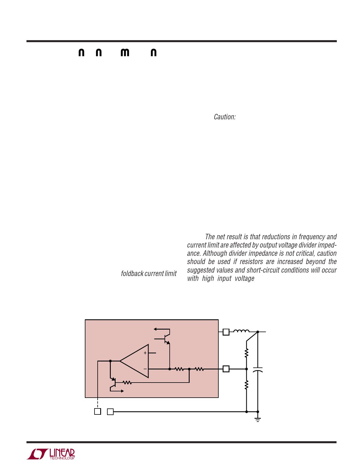
In addition to lower switching frequency, the LT1374 also
operates at lower switch current limit when the feedback
pin voltage drops below 1.7V. Q2 in Figure 2 performs this
function by clamping the VC pin to a voltage less than its
normal 2.1V upper clamp level. This foldback current limit
greatly reduces power dissipation in the IC, diode and
inductor during short-circuit conditions. External synchro-
nization is also disabled to prevent interference with
foldback operation. Again, it is nearly transparent to the
user under normal load conditions. The only loads that may
be affected are current source loads which maintain full
load current with output voltage less than 50% of final value.
In these rare situations the feedback pin can be clamped
above 1.5V with an external diode to defeat foldback cur-
rent limit. Caution: clamping the feedback pin means that
frequency shifting will also be defeated, so a combination
of high input voltage and dead shorted output may cause
the LT1374 to lose control of current limit.
The internal circuitry which forces reduced switching
frequency also causes current to flow out of the feedback
pin when output voltage is low. The equivalent circuitry is
shown in Figure 2. Q1 is completely off during normal
operation. If the FB pin falls below 1V, Q1 begins to
conduct current and reduces frequency at the rate of
approximately 5kHz/µA. To ensure adequate frequency
foldback (under worst-case short-circuit conditions), the
external divider Thevinin resistance must be low enough
to pull 150µA out of the FB pin with 0.6V on the pin (RDIV
≤ 4k). The net result is that reductions in frequency and
current limit are affected by output voltage divider imped-
ance. Although divider impedance is not critical, caution
should be used if resistors are increased beyond the
suggested values and short-circuit conditions will occur
with high input voltage. High frequency pickup will
increase and the protection accorded by frequency and
current foldback will decrease.
MAXIMUM OUTPUT LOAD CURRENT
Maximum load current for a buck converter is limited by
the maximum switch current rating (IP) of the LT1374.
This current rating is 4.5A up to 50% duty cycle (DC),
decreasing to 3.7A at 80% duty cycle. This is shown
graphically in Typical Performance Characteristics and as
shown in the formula below:
IP = 4.5A for DC ≤ 50%
IP = 3.21 + 5.95(DC) – 6.75(DC)2 for 50% < DC < 90%
DC = Duty cycle = VOUT/VIN
Example: with VOUT = 5V, VIN = 8V; DC = 5/8 = 0.625, and;
ISW(MAX) = 3.21 + 5.95(0.625) – 6.75(0.625)2 = 4.3A
Current rating decreases with duty cycle because the
LT1374 has internal slope compensation to prevent cur-
rent mode subharmonic switching. For more details, read
Application Note 19. The LT1374 is a little unusual in this
regard because it has nonlinear slope compensation which
gives better compensation with less reduction in current
limit.
Maximum load current would be equal to maximum
switch current for an infinitely large inductor, but with
finite inductor size, maximum load current is reduced by
one-half peak-to-peak inductor current. The following
formula assumes continuous mode operation, implying
that the term on the right is less than one-half of IP.
( )( ) IOUT(MAX) =
( )( )( ) Continuous Mode
IP −
VOUT VIN − VOUT
2 L f VIN
For the conditions above and L = 3.3µH,
(5)(8 − 5)
( ) ( IOUT MAX
)
=
4.3
−
2
3.3
•
10−
6
500
•
103
8
= 4.3 − 0.57 = 3.73A
At VIN = 15V, duty cycle is 33%, so IP is just equal to a fixed
4.5A, and IOUT(MAX) is equal to:
9
Share Link: 