PI74LPT162Q952V 查看數據表(PDF) - Pericom Semiconductor
零件编号
产品描述 (功能)
生产厂家
PI74LPT162Q952V Datasheet PDF : 5 Pages
| |||
PI74LPT162Q952
1234567890123456789012345678901212345678901234567890123456789012123456789012345678901234567839.0312V12314656-7B89i0t1R234e5g67i8s9t0e1r23e4d56T789r0a1n21s2c34e5i6v78e9r0s12
Maximum Ratings
(Above which the useful life may be impaired. For user guidelines, not tested)
Storage Temperature ............................................................... 65°Cto+150°C
Ambient Temperature with Power Applied .............................. 40°C to +85°C
Supply Voltage to Ground Potential (Inputs & Vcc Only) ......... 0.5Vto+7.0V
Supply Voltage to Ground Potential (Outputs & D/O Only) ...... 0.5Vto+7.0V
DC Input Voltage .......................................................................0.5Vto+7.0V
DC Output Current ................................................................................ 120mA
Power Dissipation .................................................................................... 1.0W
Note:
Stresses greater than those listed under MAXIMUM
RATINGS may cause permanent damage to the device.
This is a stress rating only and functional operation of
the device at these or any other conditions above
those indicated in the operational sections of this
specification is not implied. Exposure to absolute
maximum rating conditions for extended periods may
affect reliability.
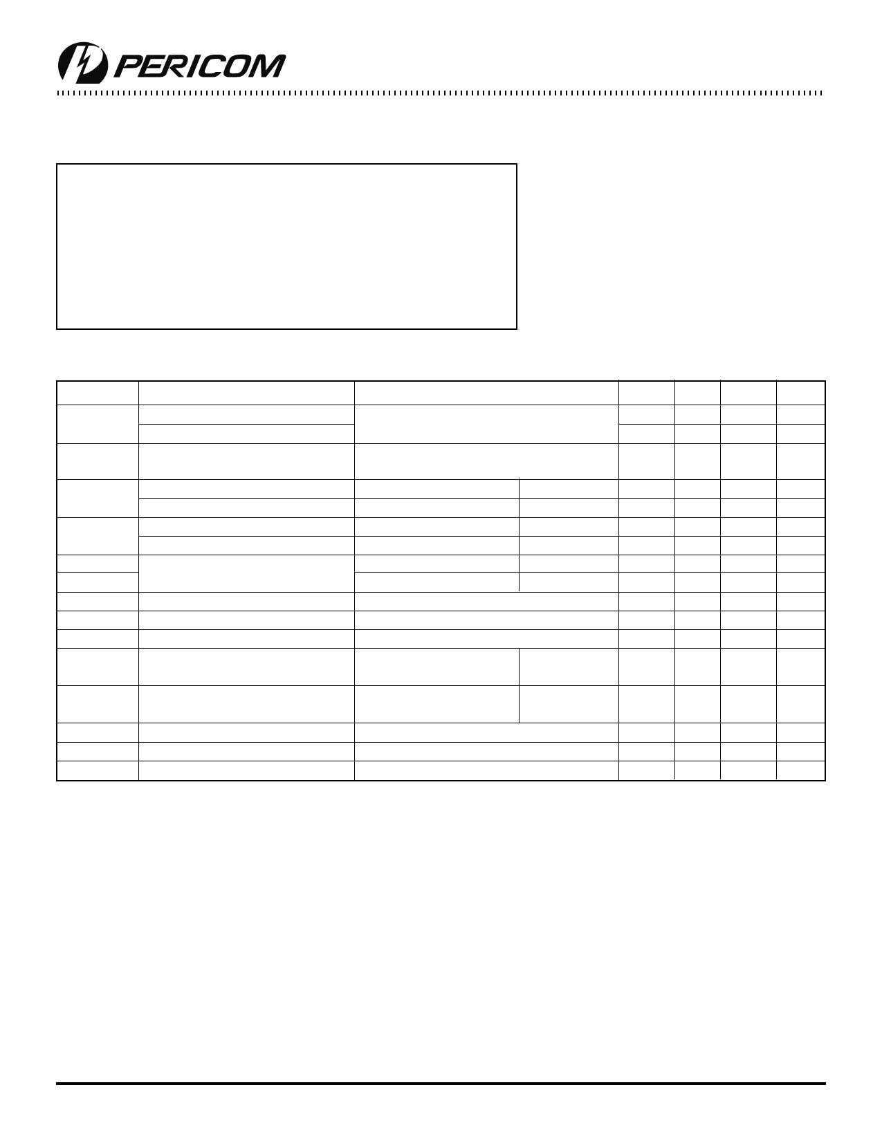
DC Electrical Characteristics (Over the Operating Range, TA = 40°C to +85°C, VCC = 2.7V to 3.6V)
Parameters
Description
Test Conditions(1)
Min. Typ(2)
VIH
Input HIGH Voltage (Input pins) Guaranteed Logic HIGH Level
2.2
Input HIGH Voltage (I/O pins)
2.0
VIL
Input LOW Voltage
Guaranteed Logic LOW Level
0.5
(Input and I/O pins)
IIH
Input HIGH Current (Input pins) VCC= Max.
VIN = 5.5V
Input HIGH Current (I/O pins)
VCC = Max.
VIN = VCC
IIL
Input LOW Current (Input pins) VCC= Max.
VIN = GND
Input LOW Current (I/O pins)
VCC = Max.
VIN = GND
IOZH
High Impedance Output Current VCC = Max.
VOUT = 5.5V
IOZL
(3-State Output pins)
VCC = Max.
VOUT = GND
VIK
Clamp Diode Voltage
VCC = Min., IIN = 18mA
70
IODH
Output HIGH Current
VCC = 3.3V, VIN = VIH or VIL, VO = 1.5V(3)
36
IODL
Output LOW Current
VCC = 3.3V, VIN = VIH or VIL, VO = 1.5V(3)
25
VOH
Output HIGH Voltage
VCC = Min.
IOH =12.0mA 2.4
3.0
VIN = VIH or VIL
VOL
Output LOW Voltage
VCC = Min.
IOL =12.0mA
0.40
VIN = VIH or VIL
IOS
Short Circuit Current(4)
VCC = Max.(3), VOUT ≤ GND 60
85 240
IOFF
Power Down Disable
VCC = 0V, VIN or VOUT 4.5V
VH
Input Hysteresis
150
Max.
5.5
5.5
0.8
±1
±1
±1
±1
±1
±1
1.2
110
100
0.55
mA
±100
Units
V
V
V
µA
µA
µA
µA
µA
µA
V
mA
mA
V
V
µA
mV
Notes:
1. For Max. or Min. conditions, use appropriate value specified under Electrical Characteristics for the applicable device type.
2. Typical values are at Vcc = 3.3V, +25°C ambient and maximum loading.
3. Not more than one output should be shorted at one time. Duration of the test should not exceed one second.
4. This parameter is guaranteed but not tested.
5. VOH = VCC 0.6V at rated current.
3
PS8098A 02/25/97
Share Link: 