SZSMS15T1G(2019) 查看數據表(PDF) - ON Semiconductor
零件编号
产品描述 (功能)
生产厂家
SZSMS15T1G Datasheet PDF : 5 Pages
| |||
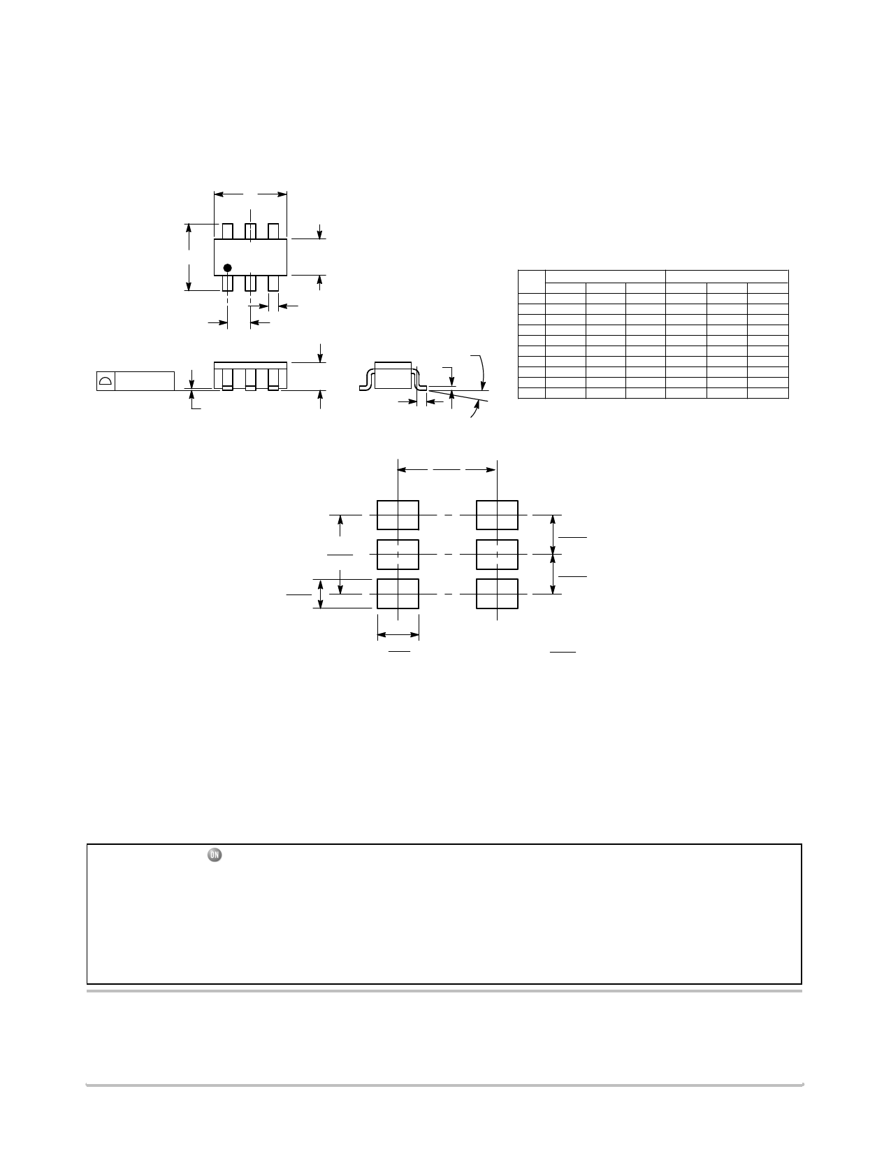
MECHANICAL CASE OUTLINE
PACKAGE DIMENSIONS
6
1
SCALE 2:1
D
65 4
HE
12 3
E
b
e
0.05 (0.002)
A
A1
SOLDERING FOOTPRINT*
2.4
0.094
SC−74
CASE 318F−05
ISSUE N
DATE 08 JUN 2012
NOTES:
1. DIMENSIONING AND TOLERANCING PER ANSI Y14.5M, 1982.
2. CONTROLLING DIMENSION: INCH.
3. MAXIMUM LEAD THICKNESS INCLUDES LEAD FINISH
THICKNESS. MINIMUM LEAD THICKNESS IS THE MINIMUM
THICKNESS OF BASE MATERIAL.
4. 318F−01, −02, −03, −04 OBSOLETE. NEW STANDARD 318F−05.
q
c
L
MILLIMETERS
DIM MIN NOM MAX
A 0.90
1.00
1.10
A1 0.01
0.06
0.10
b
0.25
0.37
0.50
c
0.10
0.18
0.26
D 2.90
3.00
3.10
E 1.30
1.50
1.70
e
0.85
0.95
1.05
L
0.20
0.40
0.60
H E 2.50
q
0°
2.75
−
3.00
10°
MIN
0.035
0.001
0.010
0.004
0.114
0.051
0.034
0.008
0.099
0°
INCHES
NOM
0.039
0.002
0.015
0.007
0.118
0.059
0.037
0.016
0.108
−
MAX
0.043
0.004
0.020
0.010
0.122
0.067
0.041
0.024
0.118
10°
GENERIC
MARKING DIAGRAM*
XXX MG
G
1.9
0.074
0.7
0.028
0.95
0.037
0.95
0.037
1.0
0.039
ǒ Ǔ SCALE 10:1
mm
inches
*For additional information on our Pb−Free strategy and soldering
details, please download the ON Semiconductor Soldering and
Mounting Techniques Reference Manual, SOLDERRM/D.
XXX
M
G
= Specific Device Code
= Date Code
= Pb−Free Package
(Note: Microdot may be in either location)
*This information is generic. Please refer to
device data sheet for actual part marking.
Pb−Free indicator, “G” or microdot “ G”,
may or may not be present.
STYLE 1:
PIN 1. CATHODE
2. ANODE
3. CATHODE
4. CATHODE
5. ANODE
6. CATHODE
STYLE 2:
PIN 1. NO CONNECTION
2. COLLECTOR
3. EMITTER
4. NO CONNECTION
5. COLLECTOR
6. BASE
STYLE 3:
PIN 1. EMITTER 1
2. BASE 1
3. COLLECTOR 2
4. EMITTER 2
5. BASE 2
6. COLLECTOR 1
STYLE 4:
PIN 1. COLLECTOR 2
2. EMITTER 1/EMITTER 2
3. COLLECTOR 1
4. EMITTER 3
5. BASE 1/BASE 2/COLLECTOR 3
6. BASE 3
STYLE 5:
PIN 1. CHANNEL 1
2. ANODE
3. CHANNEL 2
4. CHANNEL 3
5. CATHODE
6. CHANNEL 4
STYLE 6:
PIN 1. CATHODE
2. ANODE
3. CATHODE
4. CATHODE
5. CATHODE
6. CATHODE
STYLE 7:
PIN 1. SOURCE 1
2. GATE 1
3. DRAIN 2
4. SOURCE 2
5. GATE 2
6. DRAIN 1
STYLE 8:
PIN 1. EMITTER 1
2. BASE 2
3. COLLECTOR 2
4. EMITTER 2
5. BASE 1
6. COLLECTOR 1
STYLE 9:
PIN 1. EMITTER 2
2. BASE 2
3. COLLECTOR 1
4. EMITTER 1
5. BASE 1
6. COLLECTOR 2
STYLE 10:
PIN 1. ANODE/CATHODE
2. BASE
3. EMITTER
4. COLLECTOR
5. ANODE
6. CATHODE
STYLE 11:
PIN 1. EMITTER
2. BASE
3. ANODE/CATHODE
4. ANODE
5. CATHODE
6. COLLECTOR
DOCUMENT NUMBER: 98ASB42973B
DESCRIPTION: SC−74
Electronic versions are uncontrolled except when accessed directly from the Document Repository.
Printed versions are uncontrolled except when stamped “CONTROLLED COPY” in red.
PAGE 1 OF 1
ON Semiconductor and
are trademarks of Semiconductor Components Industries, LLC dba ON Semiconductor or its subsidiaries in the United States and/or other countries.
ON Semiconductor reserves the right to make changes without further notice to any products herein. ON Semiconductor makes no warranty, representation or guarantee regarding
the suitability of its products for any particular purpose, nor does ON Semiconductor assume any liability arising out of the application or use of any product or circuit, and specifically
disclaims any and all liability, including without limitation special, consequential or incidental damages. ON Semiconductor does not convey any license under its patent rights nor the
rights of others.
© Semiconductor Components Industries, LLC, 2019
www.onsemi.com
Share Link: 