ADSP-BF525KBCZ-5C2 查看數據表(PDF) - Analog Devices
零件编号
产品描述 (功能)
生产厂家
ADSP-BF525KBCZ-5C2 Datasheet PDF : 36 Pages
| |||
ADSP-BF522C/ADSP-BF523C/ADSP-BF524C/ADSP-BF525C/ADSP-BF526C/ADSP-BF527C
To allow an external device to generate the central reference
clock, apply the external clock signal directly through the XTI/
CODEC_MCLK input pin. In this configuration, the oscillator
circuit of the codec can be powered down by using the OSCPD
bit (Register R6, Bit D5) to reduce power consumption.
To accommodate applications with very high frequency master
clocks, the internal core reference clock of the codec can be set
to either CODEC_MCLK or CODEC_MCLK divided by 2. This
is enabled by adjusting the setting of the CLKDIV2 bit (Register
R8, Bit D6). The CODEC_CLKOUT pin can also drive external
clock sources with either the codec clock signal or codec clock
divided by 2 by enabling the CLKODIV2 bit (Register R8,
Bit D7).
ADC AND DAC
The codec contains a pair of oversampling Σ-Δ ADCs. The
maximum ADC full-scale input level is 1.0 Vrms when
AVDD = 3.3 V. If the input signal to the ADC exceeds this
level, data overloading occurs and causes audible distortion.
The ADC can accept analog audio input from either the stereo
line inputs or the monaural microphone input. Note that the
ADC can only accept input from a single source, so the pro-
grammer must choose either the line inputs or the microphone
input using the INSEL bit (Register R4, Bit D2). The digital data
from the ADC output, once converted, is processed using the
ADC filters.
Complementary to the Σ-Δ ADC channels, the codec contains a
pair of oversampling DACs that convert the digital audio data
from the internal DAC filters into an analog audio signal. The
DAC output can also be muted by setting the DACMU bit (Reg-
ister R5, Bit D3) in the control register.
ADC HIGH-PASS AND DAC DE-EMPHASIS FILTERS
The ADC and DAC employ separate digital filters that perform
24-bit signal processing. The digital filters are used for both
record and playback modes and are optimized for each individ-
ual sampling rate used.
For recording mode operations, the unprocessed data from the
ADC enters the ADC filters and is converted to the appropriate
sampling frequency, then is output to the digital audio interface.
For playback mode operations, the DAC filters convert the digi-
tal audio interface data to oversampled data using a sampling
rate selected by the programmer. The oversampled data is pro-
cessed by the DAC and sent to the analog output mixer by
enabling the DACSEL (Register R4, Bit D4).
Programmers have the option of setting up the device so that
any dc offset in the input source signal is automatically detected
and removed. To accomplish this, enable the digital high-pass
filter (see Table 22 on Page 30 for characteristics) contained in
the ADC digital filters by using the ADCHPD bit (Register R5,
Bit D0).
In addition, programmers can implement digital de-emphasis
by using the DEEMPH bits (Register R5, Bit D1 and Bit D2).
ANALOG AUDIO INTERFACES
The codec includes stereo single-ended line inputs and a mon-
aural microphone input to the on-board ADC. Either the line
inputs or the microphone input, but not both simultaneously,
can be connected to the ADC by setting the INSEL bit (Register
R4, Bit D2).
The codec also includes line and headphone outputs from the
on-board DAC. The line or microphone inputs can be routed
and mixed directly to the output terminals.
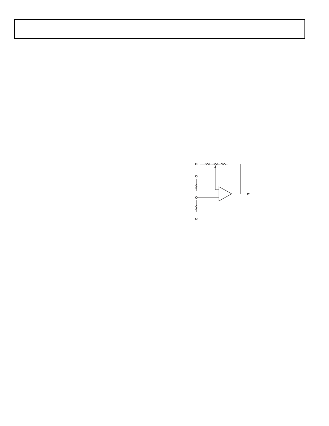
Stereo Line and Monaural Microphone Inputs
The single-ended stereo line inputs (RLINEIN and LLINEIN)
are internally biased to VMID by way of a voltage divider
between AVDD and AGND (see Figure 2). The line input signal
can be connected to the internal ADC and, if desired, routed
directly to the outputs via the bypass path by using the BYPASS
bit (Register R4, Bit D3).
RLINEIN
or
LLINEIN
AVDD
–
VMID
+
ADC
OR
BYPASS
AGND
INTERNAL CIRCUITRY
Figure 2. Line Input to ADC
The line input volume can be adjusted from –34.5 dB to +33 dB
in steps of +1.5 dB by setting the LINVOL (Register R0, Bit D0
to Bit D5) and RINVOL (Register R1, Bit D0 to Bit D5) bits. By
default the volume is independently adjustable for both right
and left line inputs. However, if the LRINBOTH or RLINBOTH
bit is programmed, both LINVOL and RINVOL are loaded with
the same value. The programmer can also set the LINMUTE
(Register R0, Bit D7) and RINMUTE (Register R1, Bit D7) bits
to mute the line input signal to the ADC.
The high impedance, low capacitance monaural microphone
input pin (MICIN, shown in Figure 3 ) has two gain stages and a
microphone bias level (MICBIAS) that is internally biased to the
VMID voltage level by way of a voltage divider between AVDD
and AGND. The microphone input signal can be connected to
the internal ADC and, if desired, routed directly to the outputs
via the sidetone path by using the SIDETONE bit (Register R4,
Bit D5).
Rev. A | Page 4 of 36 | March 2010
Share Link: 