ADSP-21368SKBPZENG ТЪЦуюІТЋИТЊџУАе№╝ѕPDF№╝Ѕ - Analog Devices
жЏХС╗Ху╝ќтЈи
С║ДтЊЂТЈЈУ┐░ (тіЪУЃй)
ућЪС║Дтјѓт«Х
ADSP-21368SKBPZENG Datasheet PDF : 48 Pages
| |||
ADSP-21368
Preliminary Technical Data
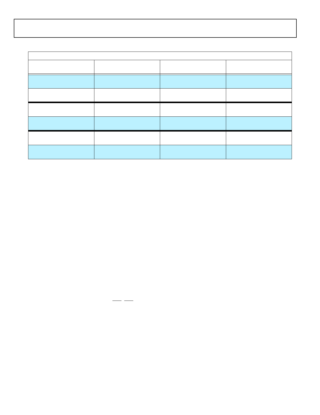
Table 2. ADSP-21368 Internal Memory Space (Continued)
IOP Registers 0x0000 0000 - 0003 FFFF
Long Word (64 bits)
Extended Precision Normal or Normal Word (32 bits)
Instruction Word (48 bits)
Reserved
0x0005 F000РђЊ0x0005 FFFF
Reserved
0x000B 4000РђЊ0x000B FFFF
Reserved
0x000B E000РђЊ 0x000B FFFF
BLOCK 1 RAM
0x0005 C000РђЊ0x0005 EFFF
BLOCK 1 RAM
0x000B 0000РђЊ0x000B 3FFF
BLOCK 1 RAM
0x000B 8000РђЊ0x000B DFFF
BLOCK 2 RAM
0x0006 0000РђЊ0x0006 0FFF
BLOCK 2 RAM
0x000C 0000РђЊ0x000C 1554
BLOCK 2 RAM
0x000C 0000РђЊ0x000C 1FFF
Reserved
0x0006 1000РђЊ 0x0006 FFFF
Reserved
0x000C 1555РђЊ0x000C 3FFF
Reserved
0x000C 2000РђЊ0x000D FFFF
BLOCK 3 RAM
0x0007 0000РђЊ0x0007 0FFF
BLOCK 3 RAM
0x000E 0000РђЊ0x000E 1554
BLOCK 3 RAM
0x000E 0000РђЊ0x000E 1FFF
Reserved
0x0007 1000РђЊ 0x0007 FFFF
Reserved
0x000E 1555РђЊ0x000F FFFF
Reserved
0x000E 2000РђЊ0x000F FFFF
Short Word (16 bits)
Reserved
0x0017 C000РђЊ0x0017 FFFF
BLOCK 1 RAM
0x0017 0000РђЊ0x0017 BFFF
BLOCK 2 RAM
0x0018 0000РђЊ0x0018 3FFF
Reserved
0x0018 4000РђЊ0x001B FFFF
BLOCK 3 RAM
0x001C 0000РђЊ0x001C 3FFF
Reserved
0x001C 4000РђЊ0x001F FFFF
Using the DM bus and PM buses, with one bus dedicated to
each memory block, assures single-cycle execution with two
data transfers. In this case, the instruction must be available in
the cache.
EXTERNAL MEMORY
The External Port on the ADSP-21368 SHARC provides a high
performance, glueless interface to a wide variety of industry-
standard memory devices. The 32-bit wide bus may be used to
interface to synchronous and/or asynchronous memory devices
through the use of it's separate internal memory controllers: the
first is an SDRAM controller for connection of industry-stan-
dard synchronous DRAM devices and DIMMs (Dual Inline
Memory Module), while the second is an asynchronous mem-
ory controller intended to interface to a variety of memory
devices. Four memory select pins enable up to four separate
devices to coexist, supporting any desired combination of syn-
chronous and asynchronous device types.
SDRAM Controller
The SDRAM controller provides an interface to up to four sepa-
rate banks of industry-standard SDRAM devices or DIMMs, at
speeds up to fSCLK. Fully compliant with the SDRAM standard,
each bank can has it's own memory select line (MS0РђЊMS3), and
can be configured to contain between 16M bytes and
128M bytes of memory.
The controller maintains all of the banks as a contiguous
address space so that the processor sees this as a single address
space, even if different size devices are used in the different
banks.
A set of programmable timing parameters is available to config-
ure the SDRAM banks to support slower memory devices. The
memory banks can be configured as either 32 bits wide for max-
imum performance and bandwidth or 16 bits wide for
minimum device count and lower system cost.
The SDRAM controller address, data, clock, and command pins
can drive loads up to 30 pF. For larger memory systems, the
SDRAM controller external buffer timing should be selected
and external buffering should be provided so that the load on
the SDRAM controller pins does not exceed 30 pF.
Asynchronous Controller
The asynchronous memory controller provides a configurable
interface for up to four separate banks of memory or I/O
devices. Each bank can be independently programmed with dif-
ferent timing parameters, enabling connection to a wide variety
of memory devices including SRAM, ROM, and flash EPROM,
as well as I/O devices that interface with standard memory con-
trol lines. Bank0 occupies a 14.7M word window and banks 1, 2,
and 3 occupy a 16M word window in the processorРђЎs address
space but, if not fully populated, these windows are not made
contiguous by the memory controller logic. The banks can also
be configured as 8-bit, 16-bit, or 32-bit wide buses for ease of
interfacing to a range of memories and I/O devices tailored
either to high performance or to low cost and power.
The asynchronous memory controller is capable of a maximum
throughput of 267M bytes/sec using a 66MHz external bus
speed. Other features include 8 to 32-bit and 16 to 32-bit pack-
ing and unpacking, booting from Bank Select 1, and support for
delay line DMA.
Shared External Memory
The ADSP-21368 supports connecting to common shared
external memory with other ADSP-21368s to create shared
external bus processor systems. This support includes:
Рђб Distributed, on-chip arbitration for the shared external bus
Рђб Fixed and rotating priority bus arbitration
Рђб Bus time-out logic
Рђб Bus lock
Rev. PrA | Page 6 of 48 | November 2004
Share Link: 