IRFP22N60KPBF 查看數據表(PDF) - Vishay Semiconductors
零件编号
产品描述 (功能)
生产厂家
IRFP22N60KPBF Datasheet PDF : 11 Pages
| |||
IRFP22N60K, SiHFP22N60K
Vishay Siliconix
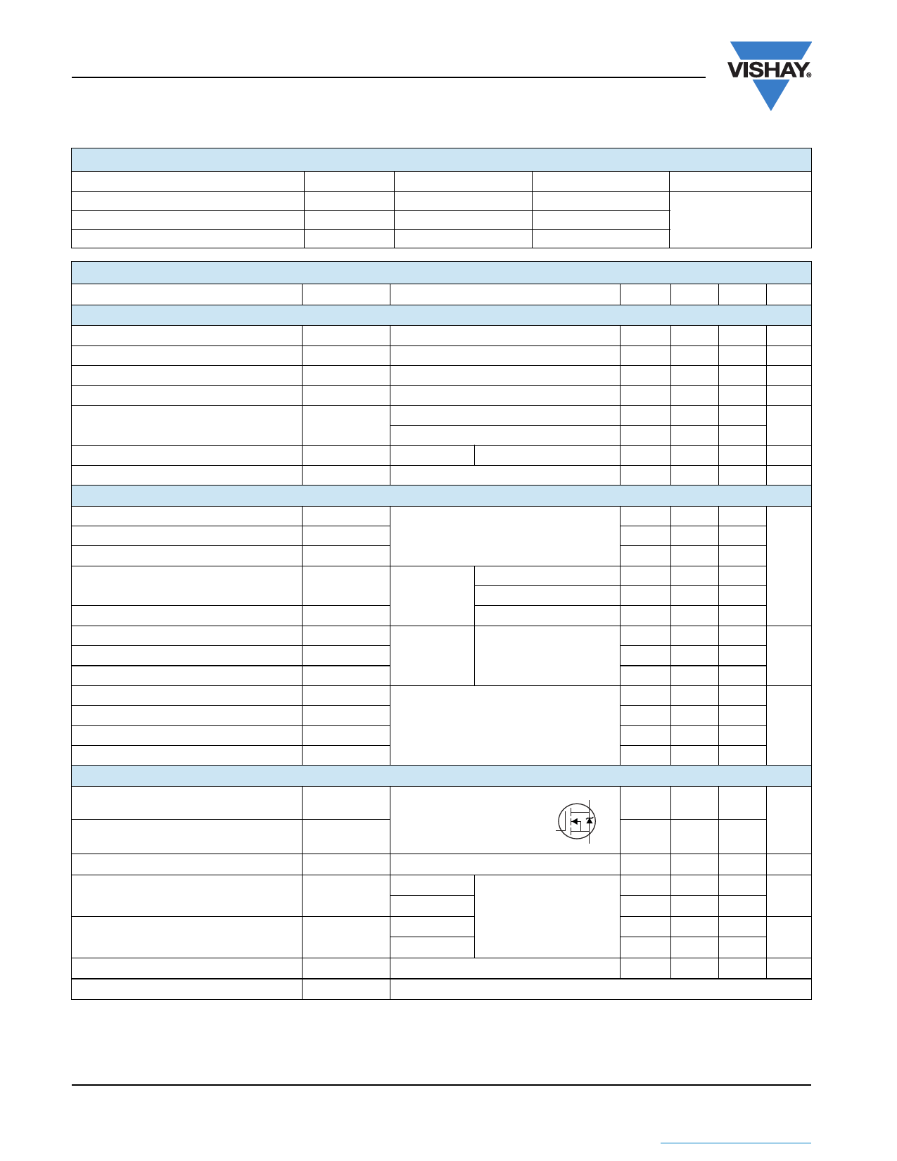
THERMAL RESISTANCE RATINGS
PARAMETER
SYMBOL
Maximum Junction-to-Ambient
Case-to-Sink, Flat, Greased Surface
Maximum Junction-to-Case (Drain)
RthJA
RthCS
RthJC
TYP.
-
0.24
-
MAX.
40
-
0.34
UNIT
°C/W
SPECIFICATIONS (TJ = 25 °C, unless otherwise noted)
PARAMETER
SYMBOL
TEST CONDITIONS
MIN. TYP. MAX. UNIT
Static
Drain-Source Breakdown Voltage
VDS Temperature Coefficient
Gate-Source Threshold Voltage
Gate-Source Leakage
Zero Gate Voltage Drain Current
Drain-Source On-State Resistance
Forward Transconductance
Dynamic
VDS
VDS/TJ
VGS(th)
IGSS
IDSS
RDS(on)
gfs
VGS = 0 V, ID = 250 μA
Reference to 25 °C, ID = 1 mAd
VDS = VGS, ID = 250 μA
VGS = ± 30 V
VDS = 600 V, VGS = 0 V
VDS = 480 V, VGS = 0 V, TJ = 125 °C
VGS = 10 V
ID = 13 Ab
VDS = 50 V, ID = 13 Ab
600
-
-
0.30
-
V
-
V/°C
3.0
-
5.0
V
-
-
± 100 nA
-
-
50
μA
-
-
250
-
0.240 0.280
11
-
-
S
Input Capacitance
Ciss
Output Capacitance
Coss
Reverse Transfer Capacitance
Crss
Output Capacitance
Coss
Effective Output Capacitance
Total Gate Charge
Gate-Source Charge
Gate-Drain Charge
Turn-On Delay Time
Rise Time
Turn-Off Delay Time
Fall Time
Drain-Source Body Diode Characteristics
Coss eff.
Qg
Qgs
Qgd
td(on)
tr
td(off)
tf
Continuous Source-Drain Diode Current
IS
Pulsed Diode Forward Currenta
ISM
VGS = 0 V,
-
VDS = 25 V,
-
f = 1.0 MHz, see fig. 5
-
VDS = 1.0 V , f = 1.0 MHz
-
VGS = 0 V VDS = 480 V , f = 1.0 MHz
-
VDS = 0 V to 480 V
-
-
VGS = 10 V
ID = 22 A, VDS = 480 V
see fig. 6 and 13b
-
-
-
VDD = 300 V, ID = 22 A,
-
Rg = 6.2, VGS = 10 V,
see fig. 10b
-
-
MOSFET symbol
showing the
D
-
integral reverse
G
p - n junction diode
-
S
3570
-
350
-
36
-
pF
4710
-
92
-
180
-
-
150
-
45
nC
-
76
26
-
99
-
ns
48
-
37
-
-
22
A
-
88
Body Diode Voltage
VSD
TJ = 25 °C, IS = 22 A, VGS = 0 Vb
-
-
1.5
V
Body Diode Reverse Recovery Time
Body Diode Reverse Recovery Charge
TJ = 25 °C
-
590 890
trr
ns
TJ = 125 °C
IF = 22 A,
-
670 1010
TJ = 25 °C
dI/dt = 100 A/μsb
-
7.2
11
Qrr
μC
TJ =1 25 °C
-
8.5
13
Reverse Recovery Current
IRRM
TJ = 25 °C
-
26
39
Forward Turn-On Time
ton
Intrinsic turn-on time is negligible (turn-on is dominated by LS and LD)
Notes
a. Repetitive rating; pulse width limited by maximum junction temperature (see fig. 11).
b. Pulse width 300 μs; duty cycle 2 %.
c. Coss eff. is a fixed capacitance that gives the same charging time as Coss while VDS is rising from 0 % to 80 % VDS.
www.vishay.com
2
Document Number: 91208
S11-0445-Rev. B, 21-Mar-11
This datasheet is subject to change without notice.
THE PRODUCT DESCRIBED HEREIN AND THIS DATASHEET ARE SUBJECT TO SPECIFIC DISCLAIMERS, SET FORTH AT www.vishay.com/doc?91000
Share Link: 