1EDF5673KXUMA1 查看數據表(PDF) - Infineon Technologies
零件编号
产品描述 (功能)
生产厂家
1EDF5673KXUMA1 Datasheet PDF : 39 Pages
| |||
1EDF5673K, 1EDF5673F, 1EDS5663H
GaN gate driver
Background and system description
The conceptual goal of the GaN EiceDRIVER™ is to provide the gate voltage of Figure 4b) or a functional
equivalent without significantly increasing driving complexity. This is achieved by slightly modifying the gate
drive waveform as depicted in Figure 4c). The "off" level after a long deadtime need not be the optimized
negative voltage -VN, it could also be the more negative level -VDDO. As these "first pulse" situations happen very
rarely compared with regular switching cycles, the resulting higher reverse voltage drop has negligible effect on
switching losses.
Although going from the 3-level signal of Figure 4b) to the 4 levels of Figure 4c) seems to increase complexity at
first sight, this is finally not true. Waveform c) can be realized in a very convenient way, if VN is generated by the
RC network as described above. Then the differential driver concept of Figure 5a) with switch control signals as
given in Figure 5b) is able to fulfil all discussed requirements with lowest effort: a single supply voltage, 4
switches and 4 connection pins are sufficient.
As mentioned, utilizing -VDDO instead of -VN only during extended "off"-phases has no impact on switching losses.
However, care has to be taken when switching on again, because CC is fully charged to VDDO in this "first pulse"
situation and no current flow is possible via the capacitive path. With the standard switching-on scheme
(open S1 / close S2) the transient current thus would be limited to the small steady-state current. To achieve a
faster turn-on, CGS will be discharged prior to the "on"-transient by switching on S3 for a short time t3 before
initiating the actual "on"-transient via S1 and S2. A t3-duration of typically 20 ns is sufficient.
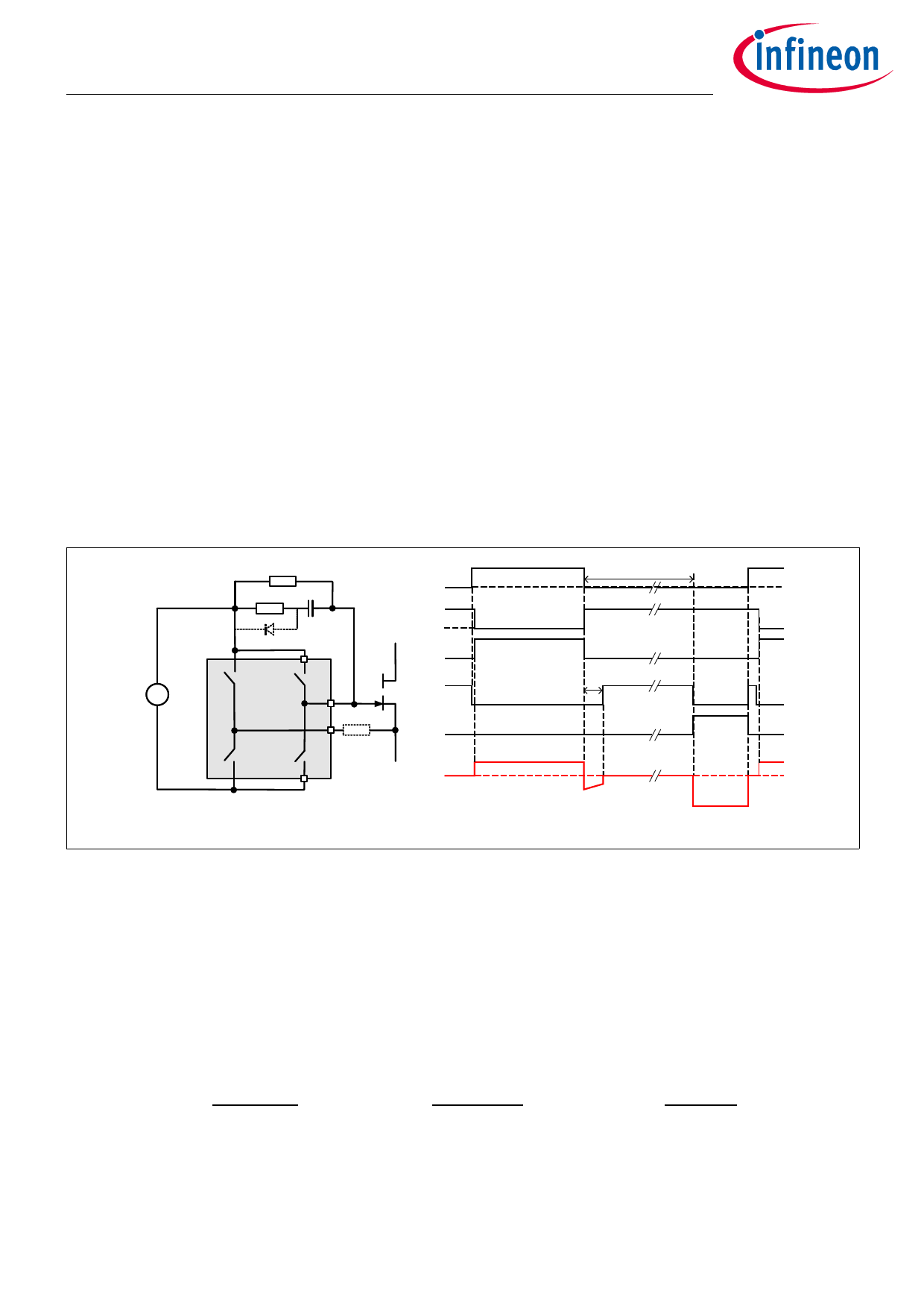
Rss
Rtr
CC
+
S1
VDDO
S2
S3
Roff
S4
a)
PWM
on
off S1
S2
S3
S4
VGS
t2 >> 1/fsw
t1
t3
-VN
-VDDO
b)
Figure 5 GaN EiceDRIVER™ concept (a) and switch control signals (b)
In the topology of Figure 5a) a single resistor Rtr is responsible for setting the maximum transient charging and
discharging current. This is often acceptable. If it is not, an additional resistor Roff with series diode in parallel with
Rtr can be used to realize different impedances for "on" and "off" transients, respectively. All relevant driving
parameters are thus easily programmable by choosing VDDO, Rss, Rtr, Roff and CC according to Equation (2.1) and
the relations
������
=
�������� − ����
������
,
������ ,������
=
��������
������ + ��������
,
�������� ,������
=
����ℎ + ����
��������
(2.2)
Final datasheet
8
Rev. 2.3
2020-10-22
Share Link: 