SI3407DV(2008) 查看數據表(PDF) - Vishay Semiconductors
零件编号
产品描述 (功能)
生产厂家
SI3407DV Datasheet PDF : 7 Pages
| |||
Si3407DV
Vishay Siliconix
New Product
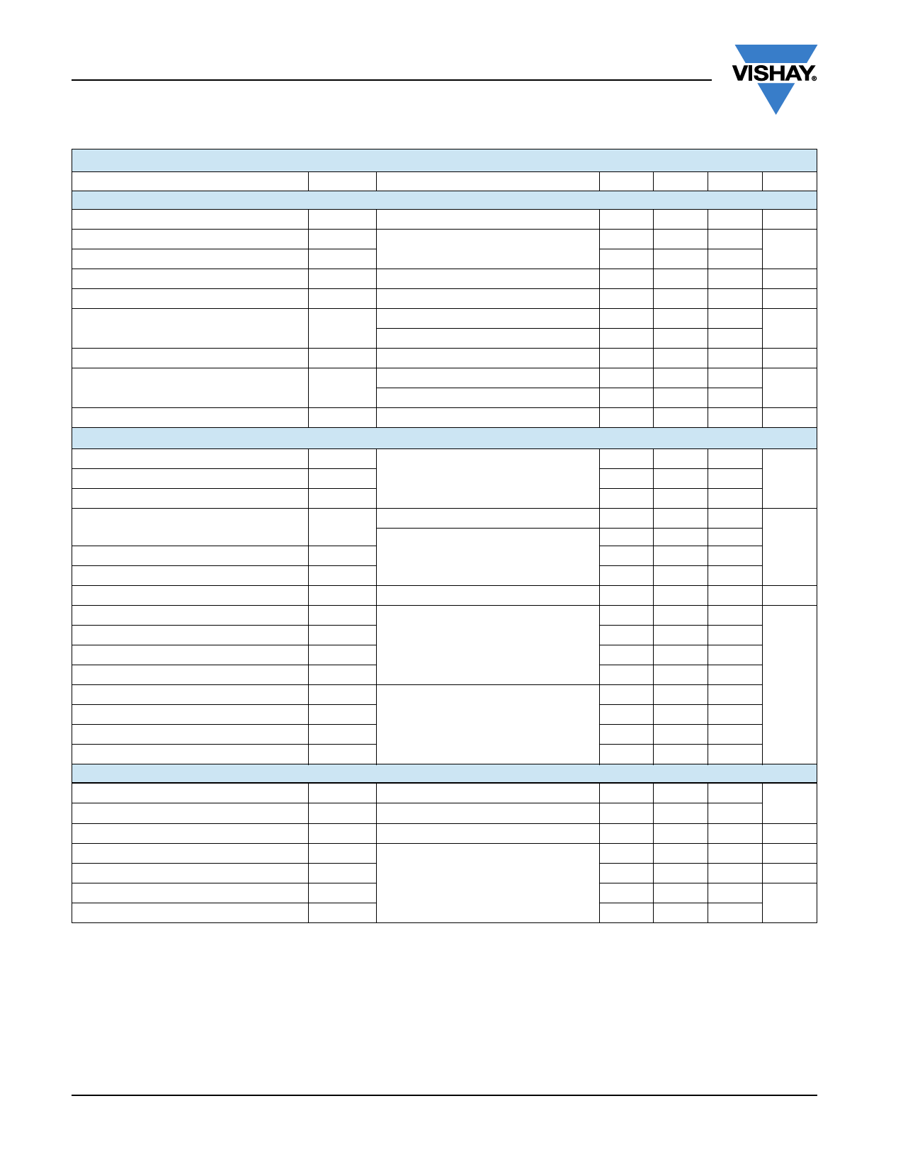
SPECIFICATIONS TJ = 25 °C, unless otherwise noted
Parameter
Symbol
Test Conditions
Static
Drain-Source Breakdown Voltage
VDS Temperature Coefficient
VGS(th) Temperature Coefficient
Gate-Source Threshold Voltage
VDS
ΔVDS/TJ
ΔVGS(th)/TJ
VGS(th)
VGS = 0 V, ID = - 250 µA
ID = - 250 µA
VDS = VGS , ID = - 250 µA
Gate-Source Leakage
IGSS
VDS = 0 V, VGS = ± 12 V
Zero Gate Voltage Drain Current
On-State Drain Currenta
IDSS
ID(on)
VDS = - 20 V, VGS = 0 V
VDS = - 20 V, VGS = 0 V, TJ = 55 °C
VDS ≤ - 5 V, VGS = - 4.5 V
Drain-Source On-State Resistancea
Forward Transconductancea
RDS(on)
gfs
VGS = - 4.5 V, ID = - 7.5 A
VGS = - 2.5 V, ID = - 6.4 A
VDS = - 10 V, ID = - 7.5 A
Dynamicb
Input Capacitance
Ciss
Output Capacitance
Coss
VDS = - 10 V, VGS = 0 V, f = 1 MHz
Reverse Transfer Capacitance
Crss
Total Gate Charge
Qg
VDS = - 10 V, VGS = - 10 V, ID = - 7.5 A
Gate-Source Charge
Gate-Drain Charge
Qgs
VDS = - 10 V, VGS = - 4.5 V, ID = - 7.5 A
Qgd
Gate Resistance
Rg
f = 1 MHz
Turn-on Delay Time
td(on)
Rise Time
Turn-Off Delay Time
tr
td(off)
VDD = - 10 V, RL = 1.7 Ω
ID ≅ - 6.0 A, VGEN = - 10 V, Rg = 1 Ω
Fall Time
tf
Turn-on Delay Time
td(on)
Rise Time
Turn-Off Delay Time
tr
td(off)
VDD = - 10 V, RL = 1.7 Ω
ID ≅ - 6.0 A, VGEN = - 4.5 V, Rg = 1 Ω
Fall Time
tf
Drain-Source Body Diode Characteristics
Continuous Source-Drain Diode Current
IS
TC = 25 °C
Pulse Diode Forward Currenta
ISM
Body Diode Voltage
VSD
IS = - 6.0 A
Body Diode Reverse Recovery Time
trr
Body Diode Reverse Recovery Charge
Reverse Recovery Fall Time
Qrr
ta
IF = 6.0 A, di/dt = 100 A/µs, TJ = 25 °C
Reverse Recovery Rise Time
tb
Notes:
a. Pulse test; pulse width ≤ 300 µs, duty cycle ≤ 2 %.
b. Guaranteed by design, not subject to production testing.
Min.
- 20
- 0.65
- 25
1.3
Typ. Max.
-18.7
3.7
- 1.5
± 100
-1
- 10
0.0200
0.0310
25
0.0240
0.0327
1670
335
284
42
63
21
32
6
5
6.5
13
8
16
11
17
65
98
39
59
32
48
62
93
53
80
38
57
- 0.8
37
22
12
25
- 3.5
- 25
- 1.2
56
33
Unit
V
mV/°C
V
nA
µA
A
Ω
S
pF
nC
Ω
ns
A
V
ns
nC
ns
Stresses beyond those listed under “Absolute Maximum Ratings” may cause permanent damage to the device. These are stress ratings only, and functional operation
of the device at these or any other conditions beyond those indicated in the operational sections of the specifications is not implied. Exposure to absolute maximum
rating conditions for extended periods may affect device reliability.
www.vishay.com
2
Document Number: 69987
S-80673-Rev. A, 31-Mar-08
Share Link: 