BR24T256FJ-WGTR_ 查看數據表(PDF) - ROHM Semiconductor
零件编号
产品描述 (功能)
生产厂家
BR24T256FJ-WGTR_ Datasheet PDF : 22 Pages
| |||
BR24T□□□□Series
Technical Note
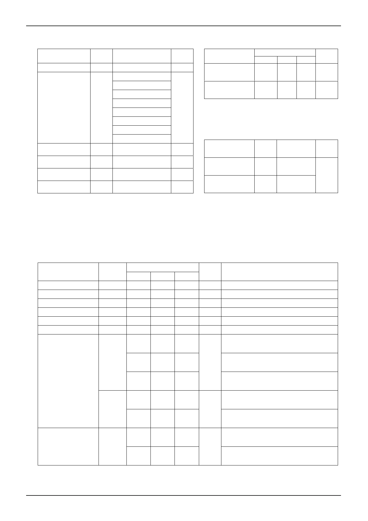
●Absolute maximum ratings (Ta=25℃)
Parameter
Symbol
Ratings
●Memory cell characteristics (Ta=25℃, Vcc=1.7~
5.5V)
Unit
Parameter
Limits
Min. Typ. Max
Unit
Impressed voltage VCC
-0.3~+6.5
450 (SOP8)*1
V
Number of data
rewrite times *1
1,000,000 -
- Times
450 (SOP-J8)*2
300 (SSOP-B8)*3
Data hold years *1 40
- - Years
Permissible
dissipation
330 (TSSOP-B8)*4
Pd
310 (TSSOP-B8J)*5 mW
*1Not 100% TESTED
310 (MSOP8) *6
300 (VSON008X2030) *7
800 (DIP-T8)*8
●Recommended operating conditions
Storage
temperature range
Tstg
-65~+150
℃
Action
temperature range
Topr
-40~+85
℃
Terminal voltage
‐
-0.3~Vcc+1.0*9
V
Parameter Symbol Ratings
Unit
Power source
voltage
Vcc
1.7~5.5
V
Junction
temperature *10
Tjmax
150
℃
*1,*2 When using at Ta=25℃ or higher 4.5mW to be reduced per 1℃.
*3,*7 When using at Ta=25℃ or higher 3.0mW to be reduced per 1℃.
*4 When using at Ta=25℃ or higher 3.3mW to be reduced per 1℃.
*5, *6 When using at Ta=25℃ or higher 3.1mW to be reduced per 1℃.
*8 When using at Ta=25℃ or higher 8.1mW to be reduced per 1℃.
*9 The Max value of Terminal Voltage is not over 6.5V.
When the pulse width is 50ns or less, the Min value of
Terminal Voltage is not under -1.0V. (BR24T16/32/64/128/256/512/1M-W)
the Min value of Terminal Voltage is not under -0.8V. (BR24T01/02/04/08-W)
*10 Junction temperature at the storage condition.
Input voltage
VIN
0~Vcc
●Electrical characteristics (Unless otherwise specified, Ta=-40~+85℃, VCC=1.7~5.5V)
Parameter
Limits
Symbol
Unit
Min. Typ. Max.
Conditions
“H” input voltage 1
“L” input voltage 1
VIH1 0.7Vcc - Vcc+1.0 V
VIL1
-0.3*2
- 0.3Vcc V
“L” output voltage 1
VOL1
-
-
0.4
V IOL=3.0mA, 2.5V≦Vcc≦5.5V (SDA)
“L” output voltage 2
VOL2
-
-
0.2
V IOL=0.7mA, 1.7V≦Vcc<2.5V (SDA)
Input leak current
ILI
-1
-
1
µA VIN=0~Vcc
Output leak current
ILO
-1
-
1
µA
-
-
2.0
ICC1
-
-
2.5
mA
Current consumption
at action
-
-
4.5
-
-
0.5
ICC2
mA
-
-
2.0
Standby current
-
-
2.0
ISB
µA
-
-
3.0
○ Radiation resistance design is not made.
*1 BR24T512/1M-W is a target value because it is developing.
*2 When the pulse width is 50ns or less, it is -1.0V. (BR24T16/32/64/128/256/512/1M-W)
When the pulse width is 50ns or less, it is -0.8V. (BR24T01/02/04/08-W)
VOUT=0~Vcc (SDA)
Vcc=5.5V,fSCL=400kHz, tWR=5ms,
Byte write, Page write
BR24T01/02/04/08/16/32/64-W
Vcc=5.5V,fSCL=400kHz, tWR=5ms,
Byte write, Page write
BR24T128/256-W
Vcc=5.5V,fSCL=400kHz, tWR=5ms,
Byte write, Page write
BR24T512/1M-W
Vcc=5.5V,fSCL=400kHz
Random read, current read, sequential read
BR24T01/02/04/08/16/32/64/128/256-W
Vcc=5.5V,fSCL=400kHz
Random read, current read, sequential read
BR24T512/1M-W
Vcc=5.5V, SDA・SCL=Vcc
A0,A1,A2=GND,WP=GND
BR24T01/02/04/08/16/32/64/128/256-W
Vcc=5.5V, SDA・SCL=Vcc
A0, A1, A2=GND, WP=GND
BR24T512/1M-W
www.rohm.com
© 2011 ROHM Co., Ltd. All rights reserved.
2/21
2011.03 - Rev.A
Share Link: 