MB39C014 查看數據表(PDF) - Cypress Semiconductor
零件编号
产品描述 (功能)
生产厂家
MB39C014 Datasheet PDF : 32 Pages
| |||
MB39C014
5. Function of Each Block
5.1 PWM Logic Control Circuit
The built-in P-ch and N-ch MOS FETs are controlled for synchronization rectification according to the frequency (2.0 MHz/3.2 MHz)
oscillated from the built-in oscillator (square wave oscillation circuit).
5.2 IOUT Comparator Circuit
This circuit detects the current (ILX) which flows to the external inductor from the built-in P-ch MOS FET.
By comparing VIDET obtained through I-V conversion of peak current IPK of ILX with the Error Amp output, the built-in P-ch MOS FET is
turned off via the PWM Logic Control circuit.
5.3 Error Amp Phase Compensation Circuit
This circuit compares the output voltage to reference voltages such as VREF. This IC has a built-in phase compensation circuit that
is designed to optimize the operation of this IC. This needs neither to be considered nor addition of a phase compensation circuit and
an external phase compensation device.
5.4 VREF Circuit
A high accuracy reference voltage is generated with BGR (bandgap reference) circuit. The output voltage is 1.20 V (Typ).
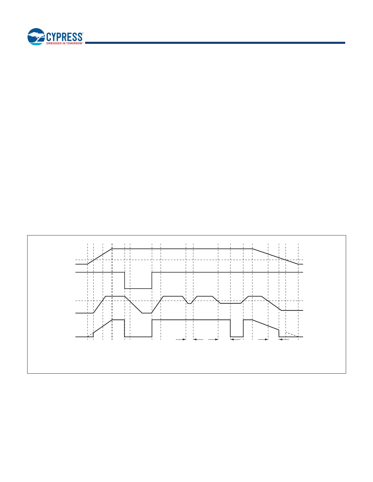
5.5 POWERGOOD Circuit
The POWERGOOD circuit monitors the voltage at the OUT pin. The POWERGOOD pin is open drain output.
Use the pin with pull-up using the external resistor in the normal operation.
When the CTL is at the H level, the POWERGOOD pin becomes the H level. However, if the output voltage drops because of over
current and etc, the POWERGOOD pin becomes the L level.
Timing Chart Example : (POWERGOOD Pin Pulled Up to VIN)
VIN
CTL
VOUT
POWERGOOD
(pull up to VIN)
VUVLO
VOUT × 97%
tDLYPG or less
tDLYPG
tDLYPG
VUVLO : UVLO threshold voltage
tDLYPG : POWERGOOD delay time
Document Number: 002-08361 Rev. *C
Page 7 of 32
Share Link: 