MB39C014 查看數據表(PDF) - Cypress Semiconductor
零件编号
产品描述 (功能)
生产厂家
MB39C014 Datasheet PDF : 32 Pages
| |||
MB39C014
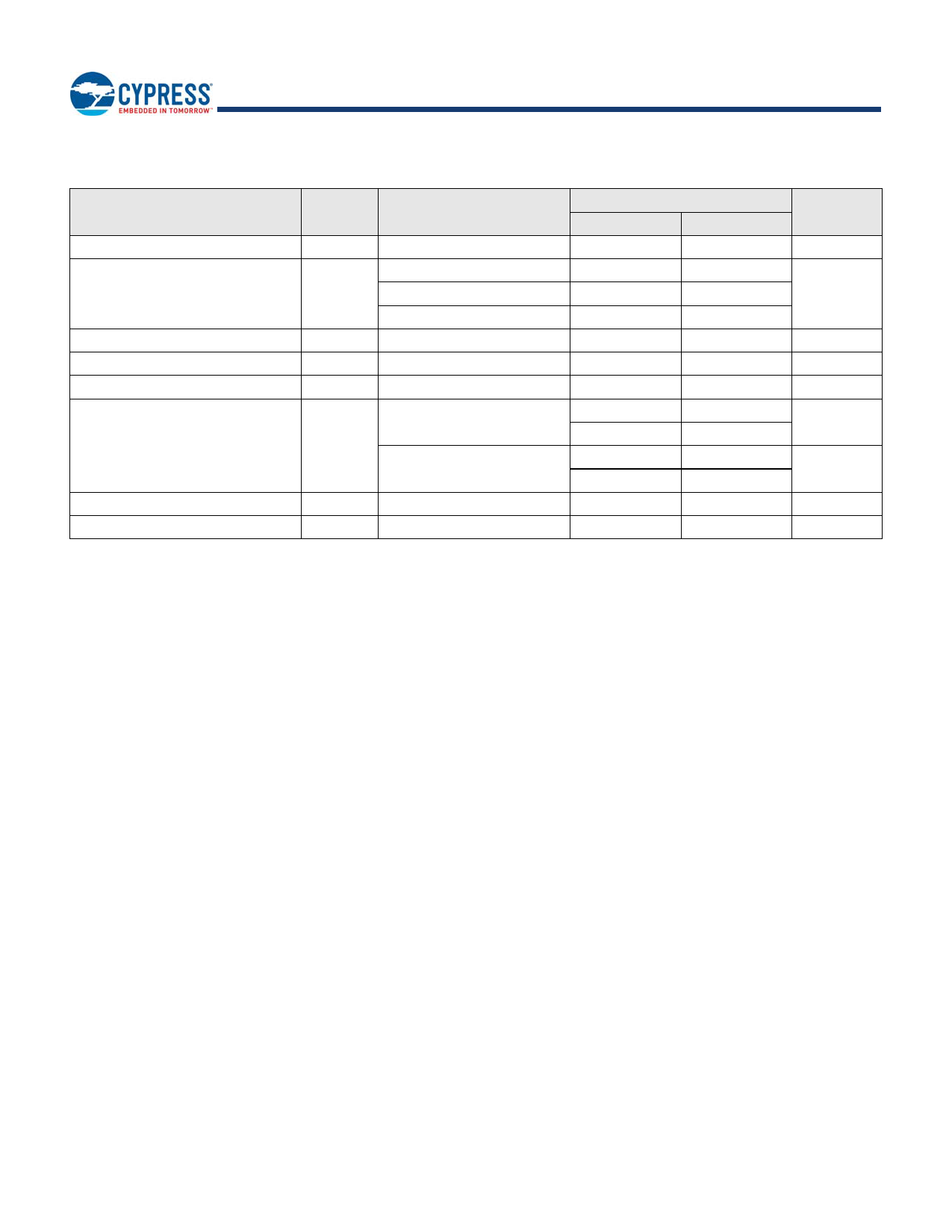
6. Absolute Maximum Ratings
Parameter
Power supply voltage
Signal input voltage
POWERGOOD pull-up voltage
LX voltage
LX peak current
Power dissipation
Operating ambient temperature
Storage temperature
Symbol
Condition
VDD
VISIG
VIPG
VLX
IPK
VDD pin
OUT pin
CTL, MODE, FSEL pins
VREFIN pin
POWERGOOD pin
LX pin
ILX
Ta ≤ + 25°C
PD
Ta = + 85 °C
Ta
—
TSTG
—
Min
− 0.3
− 0.3
− 0.3
− 0.3
− 0.3
− 0.3
—
—
—
—
—
− 40
− 55
Rating
Max
+ 6.0
VDD + 0.3
VDD + 0.3
VDD + 0.3
+ 6.0
VDD + 0.3
1.8
2632*1, *2, *3
980*1, *2, *4
1053*1, *2, *3
392*1, *2, *4
+ 85
+ 125
+ + *1 : Power dissipation value between 25°C and 85°C is obtained by connecting these two points with a straight line
*2 : When mounted on a four- layer epoxy board of 11.7 cm × 8.4 cm
*3 : Connection at exposure pad with thermal via. (Thermal via 4 holes)
*4 : Connection at exposure pad, without a thermal via.
Unit
V
V
V
V
A
mW
mW
°C
°C
Notes:
■ The use of negative voltages below − 0.3 V to the GND pin may create parasitic transistors on LSI lines, which can cause abnormal
operation.
■ This device can be damaged if the LX pin is short-circuited to VDD or GND.
■ Take measures not to keep the FSEL pin falling below the GND potential of this IC as much as possible.
In addition to erroneous operation, the IC may latch up and destroy itself if 110 mA or more current flows from this pin.
WARNING: Semiconductor devices can be permanently damaged by application of stress (voltage, current, temperature, etc.) in
excess of absolute maximum ratings. Do not exceed these ratings.
Document Number: 002-08361 Rev. *C
Page 9 of 32
Share Link: 