MAX690C 查看數據表(PDF) - Maxim Integrated
零件编号
产品描述 (功能)
生产厂家
MAX690C Datasheet PDF : 18 Pages
| |||
MAX690–MAX695
Microprocessor Supervisory Circuits
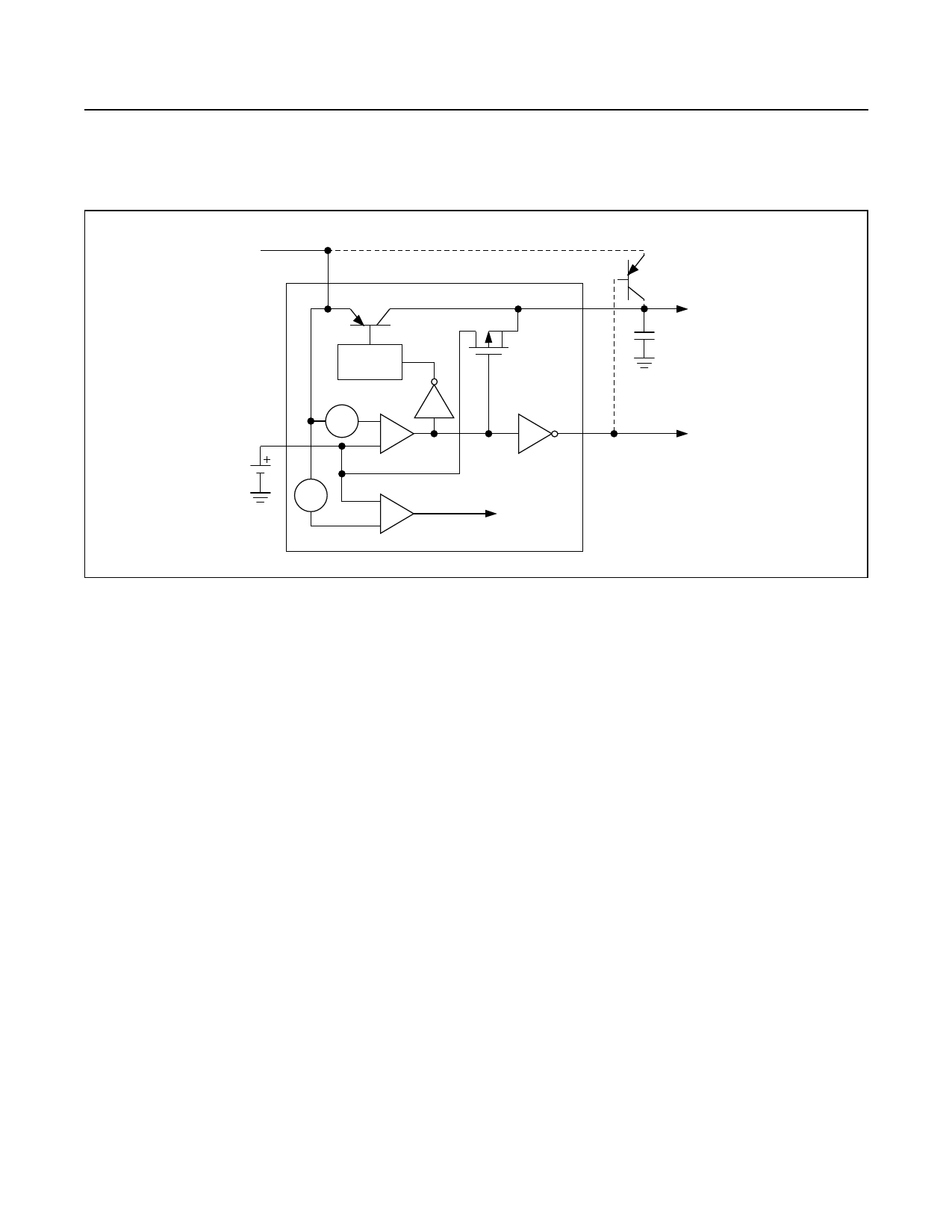
VCC
+5V
VCC
BASE DRIVE
VOUT
P CHANNEL
MOSFET
TO CMOS
RAM AND
REALTIME
CLOCK
0.1F VCC IN
3V
BATTERY
INPUT
100
mV
-
700
mV +
+
BATT ON
-
(MAX691, MAX693, MAX695 ONLY)
+
LOW IQ MODE
INTERNAL
SHUTDOWN
-
SELECT
SIGNAL WHEN
VBATT > VCC + 0.7V
Figure 4. Battery-Switchover Block Diagram
Reset Output
RESET is an active-low output which goes low when-
ever VCC falls below 4.5V (MAX690/MAX691/MAX694/
MAX695) or 4.25V (MAX692/MAX693). It will remain low
until VCC rises above 4.75V (MAX690/691/694/695) or 4.5V
(MAX692/MAX693) for milliseconds*. See Figures 5 and 6.
The guaranteed minimum and maximum thresholds of
MAX690/MAX691/MAX694/MAX695 are 4.5V and 4.75V,
while the guaranteed thresholds of the MAX692/MAX693
are 4.25V and 4.5V. The MAX690/MAX691/MAX694/
MAX695 is compatible with 5V supplies with a +10%, -5%
tolerance while the MAX692/MAX693 is compatible with
5V ±10% supplies. The reset threshold comparator has
approximately 50mV of hysteresis, with a nominal thresh-
old of 4.65V in the MAX690/MAX691/MAX694/MAX695,
and 4.4V in the MAX692/MAX693.
The response time of the reset voltage comparator is
about 100µs. VCC should be bypassed to ensure that
glitches do not activate the RESET output.
RESET also goes low if the watchdog timer is enabled
and WDI remains either high or low longer than the watch-
dog timeout period. RESET has an internal 3µA pullup,
and can either connect to and open collector Reset bus
or directly drive a CMOS gate without and external pullup
resistor.
*200ms for MAX694 and MAX695
CE Gating and RAM Write Protection
The MAX691/MAX693/MAX695 use two pins to control
the Chip Enable or Write inputs of CMOS RAMs. When
VCC is +5V, CE OUT is a buffered replica of CE IN, with
a 50ns propagation delay. If VCC input falls below 4.65V
(4.5V min, 4.75V max) an internal gate forces CE OUT
high, independent of CE IN. The MAX693 CE OUT goes
high whenever VCC is below 4.4V (4.25V min, 4.5V max).
The CE output of both devices is also forced high when
VCC is less than VBATT. (See Figure 5.)
CE OUT typically drives the CE, CS, or Write input of
battery backed up CMOS RAM. This ensures the integ-
rity of the data in memory by preventing write operations
when VCC is at and invalid level. Similar protection of
EEPROMs can be achieved by using the CE OUT to
drive the Store or Write inputs of an EEPROM, EAROM,
or NOVRAM.
If the 50ns typical propagation delay of CE OUT is too
long, connect CE IN to GND and use the resulting CE
OUT to control a high speed external logic gate. A second
alternative is to AND the LOW LINE output with the CE or
WR signal. An external logic gate and the RESET output
of the MAX690/MAX692/MAX694 can also be used for
CMOS RAM write protection.
www.maximintegrated.com
Maxim Integrated │ 9
Share Link: 