MC14489 查看數據表(PDF) - Motorola => Freescale
零件编号
产品描述 (功能)
生产厂家
MC14489 Datasheet PDF : 20 Pages
| |||
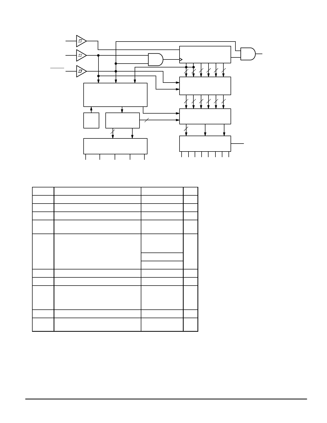
BLOCK DIAGRAM
12
DATA IN
11
CLOCK
ENABLE 10
BitGrabber
CONFIGURATION REGISTER
8 BITS
D 24–1/2–STAGE
SHIFT REGISTER
C
4 44 44 4
BitGrabber
DISPLAY REGISTER
24 BITS
4 44 4 4 4
18
DATA OUT
PIN 3 = VDD
PIN 14 = VSS
POR
OSCILLATOR AND 5
CONTROL LOGIC
5
BLANK
NIBBLE MUX AND
DECODER ROM
7 a TO g h
DIM/BRIGHT
BANK SWITCHES (FETs)
ANODE DRIVERS
(CURRENT SOURCES)
8 Rx
7 6 5 4 2 1 20 19
9
13
15
16
17
BANK 1 BANK 2 BANK 3 BANK 4 BANK 5
a b c de f g h
ÁÁÁÁÁÁÁÁÁÁÁÁÁÁÁÁÁÁÁÁÁÁÁÁÁÁÁÁÁÁÁÁÁÁÁÁÁÁÁÁÁÁÁÁ MAXIMUM RATINGS* (Voltages Referenced to VSS)
ÁÁÁÁÁÁÁÁÁÁÁÁÁÁÁÁÁÁÁÁÁÁ Symbol
Parameter
Value
Unit
ÁÁÁÁÁÁÁÁÁÁÁÁÁÁÁÁÁÁÁÁÁÁ VDD
ÁÁÁÁÁÁÁÁÁÁÁÁÁÁÁÁÁÁÁÁÁÁ Vin
ÁÁÁÁÁÁÁÁÁÁÁÁÁÁÁÁÁÁÁÁÁÁ Vout
ÁÁÁÁÁÁÁÁÁÁÁÁÁÁÁÁÁÁÁÁÁÁÁÁÁÁÁÁÁÁÁÁÁÁÁÁÁÁÁÁÁÁÁÁ Iin
DC Supply Voltage
DC Input Voltage
DC Output Voltage
DC Input Current — per Pin
(Includes Pin 8)
– 0.5 to + 6.0
V
– 0.5 to VDD + 0.5 V
– 0.5 to VDD + 0.5 V
± 15
mA
ÁÁÁÁÁÁÁÁÁÁÁÁÁÁÁÁÁÁÁÁÁÁ Iout DC Output Current —
mA
Pins 1, 2, 4 – 7, 19, 20 Sourcing
– 40
ÁÁÁÁÁÁÁÁÁÁÁÁÁÁÁÁÁÁÁÁÁÁ Sinking
10
ÁÁÁÁÁÁÁÁÁÁÁÁÁÁÁÁÁÁÁÁÁÁ Pins 9, 13, 15, 16, 17 Sinking
320
ÁÁÁÁÁÁÁÁÁÁÁÁÁÁÁÁÁÁÁÁÁÁ Pin 18
± 15
ÁÁÁÁÁÁÁÁÁÁÁÁÁÁÁÁÁÁÁÁÁÁ IDD, ISS DC Supply Current, VDD and VSS Pins
ÁÁÁÁÁÁÁÁÁÁÁÁÁÁÁÁÁÁÁÁÁÁ TJ
Chip Junction Temperature
ÁÁÁÁÁÁÁÁÁÁÁÁÁÁÁÁÁÁÁÁÁÁÁÁÁÁÁÁÁÁÁÁÁÁÁÁÁÁÁÁÁÁÁÁÁÁÁÁÁÁÁÁÁÁÁÁÁÁÁÁÁÁÁÁÁÁ RθJA
Device Thermal Resistance,
Junction–to–Ambient (see Thermal
Considerations section)
Plastic DIP
SOG Package
± 350
– 40 to + 130
90
100
mA
°C
°C/W
ÁÁÁÁÁÁÁÁÁÁÁÁÁÁÁÁÁÁÁÁÁÁ Tstg Storage Temperature
ÁÁÁÁÁÁÁÁÁÁÁÁÁÁÁÁÁÁÁÁÁÁ TL Lead Temperature, 1 mm from Case for
ÁÁÁÁÁÁÁÁÁÁÁÁÁÁÁÁÁÁÁÁÁÁ 10 Seconds
– 65 to + 150
°C
260
°C
ÁÁÁÁÁÁÁÁÁÁÁÁÁÁÁÁÁÁÁÁÁÁ * Maximum Ratings are those values beyond which damage to the device may occur.
This device contains protection circuitry to
guard against damage due to high static volt-
ages or electric fields. However, precautions
must be taken to avoid applications of any volt-
age higher than maximum rated voltages to this
high–impedance circuit. For proper operation,
Vin and Vout should be constrained to the range
VSS ≤ (Vin or Vout) ≤ VDD.
Unused inputs must always be tied to an ap-
propriate logic voltage level (e.g., either VSS or
VDD). Unused outputs must be left open.
Functional operation should be restricted to the limits in the Electrical Characteristics
tables or Pin Descriptions section.
MC14489
2
MOTOROLA
Share Link: 