VSC8122-FECQP 查看數據表(PDF) - Vitesse Semiconductor
零件编号
产品描述 (功能)
生产厂家
VSC8122-FECQP Datasheet PDF : 14 Pages
| |||
VITESSE
SEMICONDUCTOR CORPORATION
Multi-Rate SONET/SDH FEC
Clock and Data Recovery IC
Data Sheet
VSC8122-FEC
Functional Description
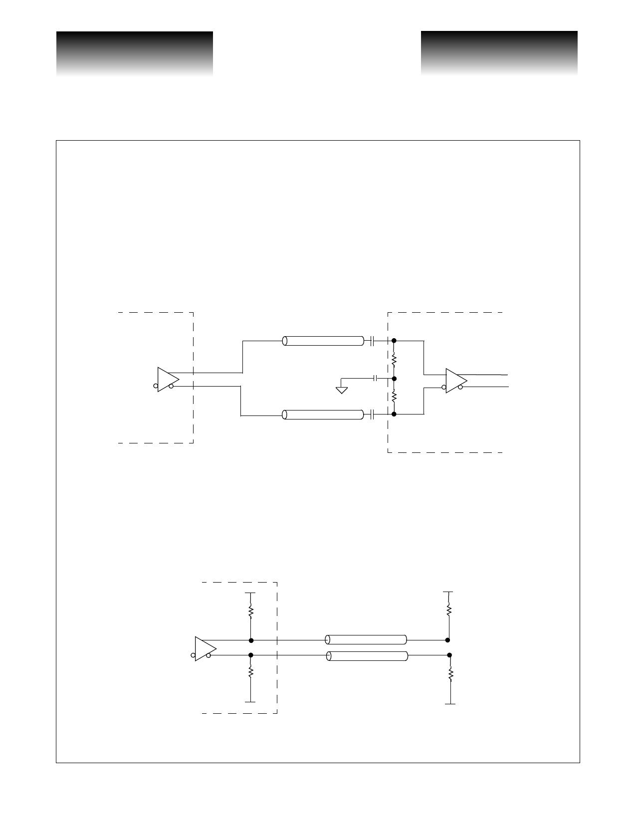
Data Input
The data input receiver is internally terminated by a center-tapped resistor network. For differential input
AC-coupling, the network is terminated to the appropriate termination voltage, VTERM through a blocking
capacitor, CAC, to ground. The input requires a differential signal with a peak-to-peak voltage on both the true
and complement of a minimum of 250mV. These inputs are required to be AC-coupled to permit use with a
variety of limiting amplifiers
Figure 1: Input Termination (AC coupled)
Limiting Amp
Zo = 50Ω
0.1 µF DI+
VSC8122-FEC
50Ω
CAC
VTERM
50Ω
Zo = 50Ω
0.1 µF DI-
High-Speed Clock and Data Outputs
The VSC8122-FEC high-speed clock and data outputs can be DC terminated, 50Ω to VCC as indicated in
Figure 2.
Figure 2: High-Speed Clock and Data Output DC Termination.
VSC8122-FEC
VCC
100Ω
CO+ / DO+
Zo = 50Ω
VCC
50Ω
CO- / DO- 100Ω
Zo = 50Ω
50Ω
VCC
VCC
Page 2
© VITESSE SEMICONDUCTOR CORPORATION • 741 Calle Plano • Camarillo, CA 93012
Tel: (800) VITESSE • FAX: (805) 987-5896 • Email: prodinfo@vitesse.com
Internet: www.vitesse.com
G52300-0, Rev 4.1
03/01/01
Share Link: 