VSC8122-FECQP 查看數據表(PDF) - Vitesse Semiconductor
零件编号
产品描述 (功能)
生产厂家
VSC8122-FECQP Datasheet PDF : 14 Pages
| |||
VITESSE
SEMICONDUCTOR CORPORATION
Multi-Rate SONET/SDH FEC
Clock and Data Recovery IC
Data Sheet
VSC8122-FEC
The NOREF output will go high to indicate that there is no signal on the REFCK input, or that the REFCK
is more than approximately 25% above or below the expected value.
Two sets of reference frequencies for the VSC8122-FEC are shown in Table 2. SONET reference clock fre-
quencies are as indicated, with Gigabit Ethernet frequencies listed in parenthesis. FEC rate frequencies are indi-
cated at rates for use with the VSC9210 FEC device operating at 2.65Gb/s. The two different sets of reference
clocks are needed since the reference clock for SONET and Gigabit Ethernet applications will be slightly differ-
ent. Internally, the VSC8122-FEC requires a 19.44MHz reference (or 19.53MHz reference for Gigabit Ether-
net).
The customer can select to provide either the 19.44MHz reference (or 19.53MHz reference for Gigabit
Ethernet), or the 2x, 4x or 8x of that reference at 38.88MHz (39.06MHz), 77.76MHz (78.13MHz) or 155MHz
(156.25MHz). For FEC rates, the customer can select the appropriate frequency as indicated in Table 2. The
REF_SEL[1:0] inputs will program the internal divider as required to use the selected REFCK frequency.
Two reference clock inputs are provided, REFCK1 and REFCK0, to allow “on the fly switching” between
SONET and Gigabit Ethernet applications if desired. Since SONET and Gigabit Ethernet require different refer-
ence clock frequencies, the VSC8122-FEC allows the user to toggle between the two reference clock frequen-
cies REFCK1 and REFCK0 to supply the appropriate input clock. REF_INPUTSEL is used to toggle between
the two reference clock input frequencies. REF_INPUTSEL= “0” selects REFCK0, REF_INPUTSEL= “1”
selects REFCK1. Either reference clock input (REFCK1, REFCK0) can be used for SONET or Gigabit Ethernet
reference frequencies. PECL levels are recommended for REFCK inputs (see Figure 4). If a reference clock is
unused, it is recommended that one of its inputs be tied to VCC through a 5.1kΩ resistor, the other one to GND
through a 5.1kΩ resistor.
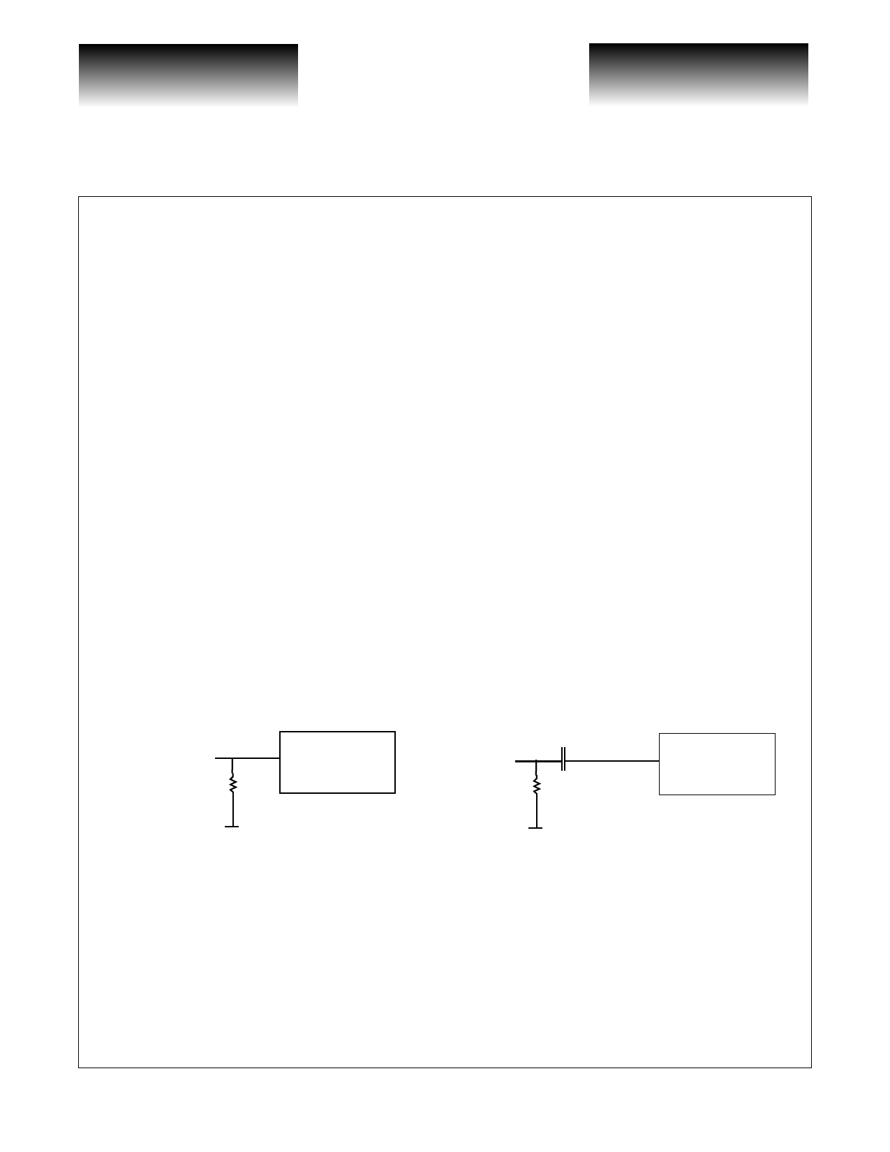
Figure 4: REFCK Input Levels
PECL Level REFCK Inputs (recommended)
NON- PECL Level REFCK Inputs
REFCK0 /
REFCK1
VSC8122-FEC
50Ω
REFCK0 /
REFCK1
0.1µf
50Ω
VSC8122-FEC
VTERM
VTERM
* VTERM can be to any power supply, as long as PECL levels are supplied to REFCK inputs.
Typically, VEE (typ. GND) is used as VTERM.
** For differential REFCK input signals, 100Ω termination between true and complement
REFCK signals can be substituted for the 50Ω to VTERM termination on each line.
Page 4
© VITESSE SEMICONDUCTOR CORPORATION • 741 Calle Plano • Camarillo, CA 93012
Tel: (800) VITESSE • FAX: (805) 987-5896 • Email: prodinfo@vitesse.com
Internet: www.vitesse.com
G52300-0, Rev 4.1
03/01/01
Share Link: 