MJE5740G(2015) 查看數據表(PDF) - ON Semiconductor
零件编号
产品描述 (功能)
生产厂家
MJE5740G Datasheet PDF : 6 Pages
| |||
MJE5740, MJE5742
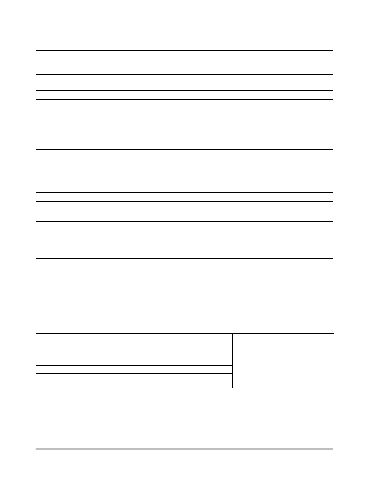
ÎÎÎÎÎÎÎÎÎÎÎÎÎÎÎÎÎÎÎÎÎÎÎÎÎÎÎÎÎÎÎÎÎ ELECTRICAL CHARACTERISTICS (TC = 25_C unless otherwise noted)
ÎÎÎÎÎÎÎÎÎÎÎÎÎÎÎÎÎÎÎÎÎÎÎÎÎÎÎÎÎÎÎÎÎ Characteristic
Symbol
Min
ÎÎÎÎÎÎÎÎÎÎÎÎÎÎÎÎÎÎÎÎÎÎÎÎÎÎÎÎÎÎÎÎÎ OFF CHARACTERISTICS (Note 2)
ÎÎÎÎÎÎÎÎÎÎÎÎÎÎÎÎÎÎÎÎÎÎÎÎÎÎÎÎÎÎÎÎÎ Collector−Emitter Sustaining Voltage
(IC = 50 mA, IB = 0)
MJE5740 VCEO(sus)
300
MJE5742
400
ÎÎÎÎÎÎÎÎÎÎÎÎÎÎÎÎÎÎÎÎÎÎÎÎÎÎÎÎÎÎÎÎÎ Collector Cutoff Current (VCEV = Rated Value, VBE(off) = 1.5 Vdc)
ÎÎÎÎÎÎÎÎÎÎÎÎÎÎÎÎÎÎÎÎÎÎÎÎÎÎÎÎÎÎÎÎÎ (VCEV = Rated Value, VBE(off) = 1.5 Vdc, TC = 100_C)
ICEV
−
−
ÎÎÎÎÎÎÎÎÎÎÎÎÎÎÎÎÎÎÎÎÎÎÎÎÎÎÎÎÎÎÎÎÎ Emitter Cutoff Current (VEB = 8 Vdc, IC = 0)
IEBO
−
ÎÎÎÎÎÎÎÎÎÎÎÎÎÎÎÎÎÎÎÎÎÎÎÎÎÎÎÎÎÎÎÎÎ SECOND BREAKDOWN
ÎÎÎÎÎÎÎÎÎÎÎÎÎÎÎÎÎÎÎÎÎÎÎÎÎÎÎÎÎÎÎÎÎ Second Breakdown Collector Current with Base Forward Biased
ÎÎÎÎÎÎÎÎÎÎÎÎÎÎÎÎÎÎÎÎÎÎÎÎÎÎÎÎÎÎÎÎÎ Clamped Inductive SOA with Base Reverse Biased
IS/b
RBSOA
ÎÎÎÎÎÎÎÎÎÎÎÎÎÎÎÎÎÎÎÎÎÎÎÎÎÎÎÎÎÎÎÎÎ ON CHARACTERISTICS (Note 2)
ÎÎÎÎÎÎÎÎÎÎÎÎÎÎÎÎÎÎÎÎÎÎÎÎÎÎÎÎÎÎÎÎÎ DC Current Gain (IC = 0.5 Adc, VCE = 5 Vdc)
(IC = 4 Adc, VCE = 5 Vdc)
hFE
50
200
ÎÎÎÎÎÎÎÎÎÎÎÎÎÎÎÎÎÎÎÎÎÎÎÎÎÎÎÎÎÎÎÎÎ Collector−Emitter Saturation Voltage (IC = 4 Adc, IB = 0.2 Adc)
VCE(sat)
−
ÎÎÎÎÎÎÎÎÎÎÎÎÎÎÎÎÎÎÎÎÎÎÎÎÎÎÎÎÎÎÎÎÎ Collector−Emitter Saturation Voltage (IC = 8 Adc, IB = 0.4 Adc)
−
ÎÎÎÎÎÎÎÎÎÎÎÎÎÎÎÎÎÎÎÎÎÎÎÎÎÎÎÎÎÎÎÎÎ Collector−Emitter Saturation Voltage (IC = 4 Adc, IB = 0.2 Adc, TC = 100_C)
−
ÎÎÎÎÎÎÎÎÎÎÎÎÎÎÎÎÎÎÎÎÎÎÎÎÎÎÎÎÎÎÎÎÎ Base−Emitter Saturation Voltage (IC = 4 Adc, IB = 0.2 Adc)
Base−Emitter Saturation Voltage (IC = 8 Adc, IB = 0.4 Adc)
ÎÎÎÎÎÎÎÎÎÎÎÎÎÎÎÎÎÎÎÎÎÎÎÎÎÎÎÎÎÎÎÎÎ Base−Emitter Saturation Voltage (IC = 4 Adc, IB = 0.2 Adc, TC = 100_C)
VBE(sat)
−
−
−
ÎÎÎÎÎÎÎÎÎÎÎÎÎÎÎÎÎÎÎÎÎÎÎÎÎÎÎÎÎÎÎÎÎ Diode Forward Voltage (Note 3) (IF = 5 Adc)
Vf
−
ÎÎÎÎÎÎÎÎÎÎÎÎÎÎÎÎÎÎÎÎÎÎÎÎÎÎÎÎÎÎÎÎÎ SWITCHING CHARACTERISTICS
ÎÎÎÎÎÎÎÎÎÎÎÎÎÎÎÎÎÎÎÎÎÎÎÎÎÎÎÎÎÎÎÎÎ Typical Resistive Load (Table 1)
ÎÎÎÎÎÎÎÎÎÎÎÎÎÎÎÎÎÎÎÎÎÎÎÎÎÎÎÎÎÎÎÎÎ Delay Time
ÎÎÎÎÎÎÎÎÎÎÎÎÎÎÎÎÎÎÎÎÎÎÎÎÎÎÎÎÎÎÎÎÎ Rise Time
ÎÎÎÎÎÎÎÎÎÎÎÎÎÎÎÎÎÎÎÎÎÎÎÎÎÎÎÎÎÎÎÎÎ Storage Time
ÎÎÎÎÎÎÎÎÎÎÎÎÎÎÎÎÎÎÎÎÎÎÎÎÎÎÎÎÎÎÎÎÎ Fall Time
(VCC = 250 Vdc, IC(pk) = 6 A
IB1 = IB2 = 0.25 A, tp = 25 ms,
Duty Cycle v 1%)
ÎÎÎÎÎÎÎÎÎÎÎÎÎÎÎÎÎÎÎÎÎÎÎÎÎÎÎÎÎÎÎÎÎ Inductive Load, Clamped (Table 1)
ÎÎÎÎÎÎÎÎÎÎÎÎÎÎÎÎÎÎÎÎÎÎÎÎÎÎÎÎÎÎÎÎÎ Voltage Storage Time
ÎÎÎÎÎÎÎÎÎÎÎÎÎÎÎÎÎÎÎÎÎÎÎÎÎÎÎÎÎÎÎÎÎÎÎÎÎÎÎÎÎÎÎÎÎÎÎÎÎÎÎÎÎÎÎÎÎÎÎÎÎÎÎÎÎÎ Crossover Time
(IC(pk) = 6 A, VCE(pk) = 250 Vdc
IB1 = 0.06 A, VBE(off) = 5 Vdc)
td
−
tr
−
ts
−
tf
−
tsv
−
tc
−
Typ
Max
Unit
−
−
Vdc
−
−
−
1
mAdc
−
5
−
75
mAdc
See Figure 6
See Figure 7
100
−
−
400
−
−
2
Vdc
−
3
−
2.2
−
2.5
Vdc
−
3.5
−
2.4
−
2.5
Vdc
0.04
−
ms
0.5
−
ms
8
−
ms
2
−
ms
4
−
ms
2
−
ms
Product parametric performance is indicated in the Electrical Characteristics for the listed test conditions, unless otherwise noted. Product
performance may not be indicated by the Electrical Characteristics if operated under different conditions.
2. Pulse Test: Pulse Width 300 ms, Duty Cycle = 2%.
3. The internal Collector−to−Emitter diode can eliminate the need for an external diode to clamp inductive loads. Tests have shown that the
Forward Recovery Voltage (Vf) of this diode is comparable to that of typical fast recovery rectifiers.
ORDERING INFORMATION
Device
MJE5740G
MJE5742G
Package
TO−220
(Pb−Free)
TO−220
(Pb−Free)
Shipping
50 Units / Rail
www.onsemi.com
2
Share Link: 