Q-67107-H5236 查看數據表(PDF) - Micronas
零件编号
产品描述 (功能)
生产厂家
Q-67107-H5236 Datasheet PDF : 154 Pages
| |||
SDA 9402/02S(A31)
Preliminary Data Sheet 02.2001
System Description
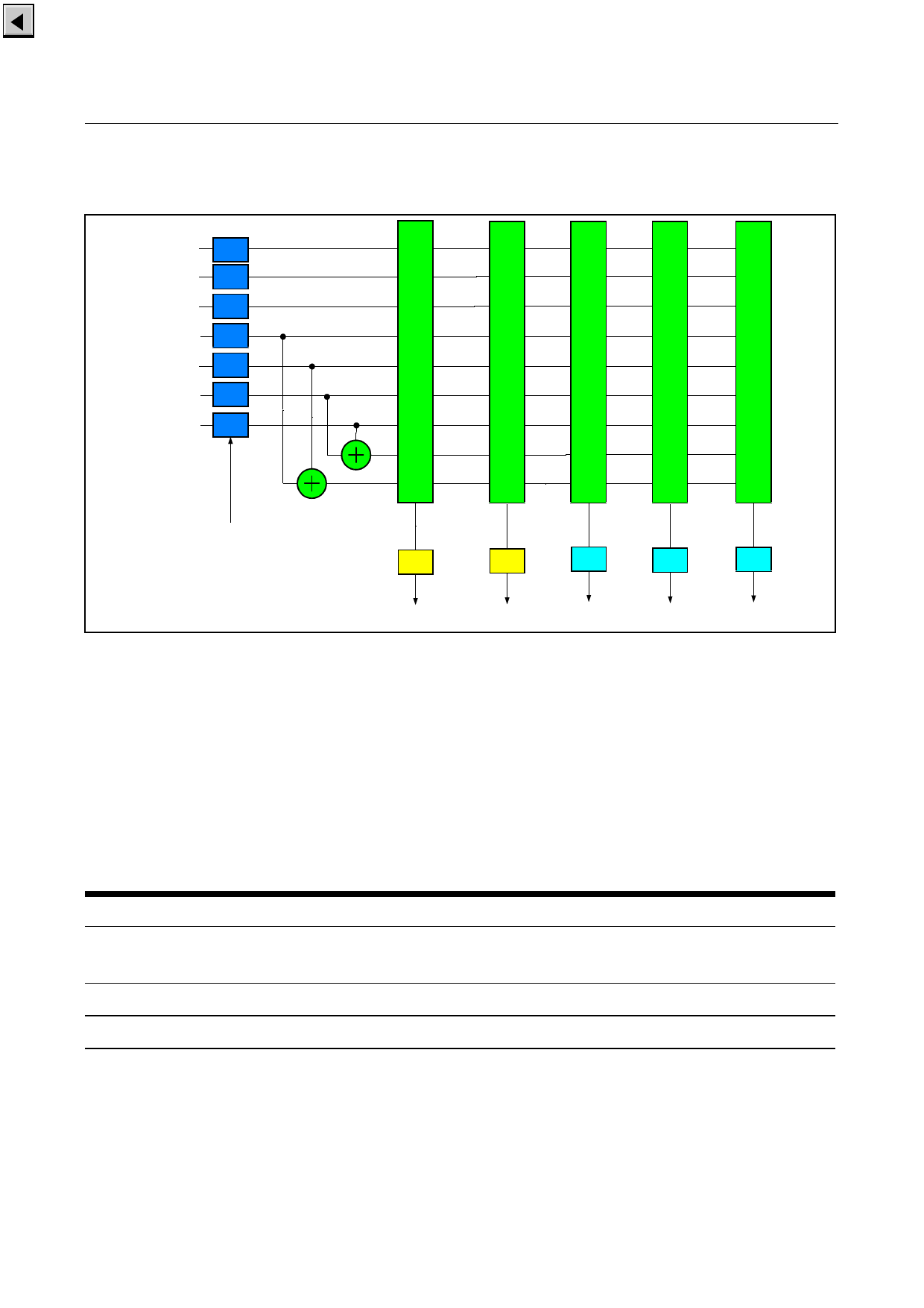
CVBS 1
C
CVBS 2
C
CVBS 3
C
CVBS 4 / Y1 C
CVBS 5 / C1 C
CVBS 6 / Y2 C
CVBS 7 / C2 C
1
1
1
1
1
/
/
/
/
/
9
9
9
9
9
Clamping pulse of ADC_CVBS1
or ADC_CVBS2.
Shifting of signal to required
input voltage range for
CVBSO1..3
Figure 5-1 Input selection
Filter
Filter
Buffer
ADC_CVBS1 ADC_CVBS2 CVBSO1
BuCffer
CVBSO2
Buffer
CVBSO3
5.1.2 Signal Magnitudes and Gain Control
To adjust to different CVBS input voltages a digitally working automatic gain control with
64 linear steps is implemented for input voltages in the range from 0.5 to 1.5Vpp. For best
signal-to-noise ratio the maximum CVBS amplitude is recommended. The AGC behavior
can be chosen from four possible modes (AGCMD):
AGCMD
00
01
10
11
AGC operation mode
AGC uses the height of the sync pulse as a reference
AGC uses the height of the sync pulse as a reference and additionally
reduces amplification when ADC overflows
AGC uses only ADC overflows
AGC is disabled and the ADC fits to the values given in AGCADJ1
Table 5- 1 AGC modes
When using the sync height, the A/D gain rises or falls depending on the incoming signal.
When using overflow detection only, the gain is set to maximum and is reduced
whenever an ’overflow’ occurs. The signal is lowpassed so that chrominance and noise
are not used for detection. The threshold can be adjusted by PWTHD. A setting of ’11’
Micronas
5-17
Share Link: 