Q-67107-H5236 查看數據表(PDF) - Micronas
零件编号
产品描述 (功能)
生产厂家
Q-67107-H5236 Datasheet PDF : 154 Pages
| |||
SDA 9402/02S(A31)
Preliminary Data Sheet 02.2001
System Description
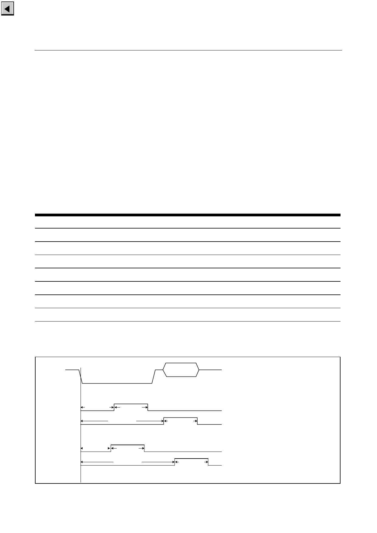
5.1.3 Clamping
The clamp timing for the analog inputs is generated from its corresponding CVBS signal.
The clamping algorithm works with a split measurement pulse and a clamping pulse. The
measurement pulse is used to detect the clamping error. The clamping pulse is used to
enable current sources for reducing the detected clamping errors. The start and length
of the measurement signal is adjustable independently for both channels (CLMPST1,
CLMPD1, CLMPST2, CLMPD2). The start and length of the clamping signal is
adjustable for both channels independently (CLMPST1S, CLMPD1S, CLMPST2S,
CLMPD2S). Clamping signals for RGB-channel are not split. Clamping for these ADC
are controlled by CLMPST2 and CLMPD2 only. Clamping can be suppressed for some
lines by CLMPLOW and CLMPHIGH to ignore copyprotection information. No external
sync signals are required.
signal
description
CLMPST1 measurement pulse start for ADC1
CLMPD1 measurement pulse duration for ADC1
CLMPST1S clamping pulse start for ADC1
CLMPD1S clamping pulse duration for ADC1
CLMPST2 measurement pulse start for ADC2 (and m/c for RGBF-ADC)
CLMPD2 measurement pulse duration for ADC2 (and m/c for RGBF-ADC)
CLMPST2S clamping pulse start for ADC2
CLMPD2S clamping pulse duration for ADC2
Table 5- 2 Clamping adjustment
sync separation input
measure
clamp
CLMPST1 CLMPD1
CLMPST1S
CLMPD1S
CLAMP1 signals
measure
clamp
CLMPST2 CLMPD2
CLMPST2S
CLMPD2S
CLAMP2 signals
Figure 5-4 Clamping signals
Micronas
5-19
Share Link: 